John Byrd has been named director of the U.S. Particle Accelerator School (USPAS). He succeeds Professor Steven Lund of Michigan State University, who has served as director since 2018.
USPAS is the nation’s premier training program in accelerator science and engineering. The school’s collaboration includes seven Department of Energy Office of Science laboratories, one DOE National Nuclear Security Administration laboratory and two universities.

USPAS is the nation’s premier training program in accelerator science and engineering. The school’s collaboration includes seven Department of Energy Office of Science laboratories, one DOE National Nuclear Security Administration laboratory and two universities.
“Being selected as the USPAS director is a true ‘circle-of-life’ moment for me,” said Byrd. “My career in accelerator science began in 1988, inspired by a USPAS course taught by Don Edwards and Mike Syphers, and it has been a privilege to witness and contribute to the field’s extraordinary development over the past three decades. It is both humbling and profoundly meaningful to now have the opportunity to give back to the community and institution that helped shape my professional life.”
After earning his Ph.D. in physics from Cornell University in 1991, Byrd spent 26 years at Lawrence Berkeley National Laboratory (LBNL), contributing to major accelerator facilities, including PEP-II at SLAC, the Advanced Light Source at LBNL, the Linac Coherent Light Source at SLAC, the Large Hadron Collider at CERN and the Free Electron Laser Radiation for Multidisciplinary Investigations at Elettra.
n 2017, he joined Argonne National Laboratory as division director for the accelerator systems division at the Advanced Photon Source (APS), leading efforts for the operation of the APS and contributing to the design, construction and commissioning of the APS upgrade. After retiring from Argonne in 2024, he worked on several industrial accelerator projects before accepting the position of USPAS director.
“The U.S. Particle Accelerator School has educated next-generation accelerator physicists and engineers for decades and through that, made sure that we can build ever better accelerators and develop new important technologies,” said Norbert Holtkamp, director of Fermi National Accelerator Laboratory.
Founded in 1981, USPAS convenes twice each year to offer a broad range of graduate-level courses through an intensive school format. USPAS offers a continually updated curriculum ranging from foundational accelerator science to advanced physics and engineering topics. In addition to meeting the workforce needs of national laboratories, the school educates students and professionals on the many applications of particle accelerators in areas such as science, medicine, security and industry. The training and documentation produced through USPAS sessions are broadly recognized for excellence and have had a profound and lasting impact on the accelerator community.
The USPAS office at Fermilab and the USPAS director are responsible for the operation and management of the school, coordinating across the entire accelerator community through the USPAS Institutional Board and the USPAS Director’s Advisory Council.
“The U.S. Particle Accelerator School has educated next-generation accelerator physicists and engineers for decades and through that, made sure that we can build ever better accelerators and develop new important technologies,”
Norbert Holtkamp, director of Fermi National Accelerator Laboratory
“I am very pleased to hear this news,” said Cameron Geddes, director of the Accelerator Technology & Applied Physics Division at Lawrence Berkeley National Laboratory and a member of the USPAS Institutional Board. “John’s distinguished research perspective will advance the vital role of the school in providing accelerator physics education not available at most universities and help him leverage the contributions of lecturers from around the community.”
“Over the past 45 years, USPAS has become a cornerstone of education and training for national laboratories that rely on accelerator-based research,” said Zhirong Huang of SLAC National Accelerator Laboratory and Stanford University, and also chair of the USPAS Curriculum Committee and the Director Search Committee. “On behalf of the national laboratory and university communities, we extend our sincere thanks to the outgoing director, Steve Lund, for his eight years of dedicated leadership at USPAS. We have also valued our work with John Byrd through his many years of teaching USPAS classes, his years of service on the USPAS Director’s Advisory Council and Curriculum Committee, and we look forward to continuing our work with him as he steps into the role of the USPAS director, furthering this vital mission.”
Particle accelerators are a critical driver of both discovery science and industry that broadly enable the mission of the U.S. Department of Energy Office of Science. As some of the most complex, large-scale systems in the world, DOE’s accelerators play a key role in DOE’s new Genesis Mission, which aims to revolutionize the nation’s science and technology output by leveraging and extending state-of-the-art artificial intelligence. Genesis will open new capabilities and horizons in accelerator science and technology. The world-class training that USPAS provides will ensure that students, scientists and industry professionals in the accelerator field are ready for that future.
“The Office of High Energy Physics has proudly supported the U.S. Particle Accelerator School since the early 1980s, recognizing its critical role in cultivating the next generation of accelerator scientists and engineers,” said Regina Rameika, associate director for the Office of High Energy Physics within DOE’s Office of Science. “Our continued investment, notably through HEP’s General Accelerator Research Development program and the Accelerator Traineeship program, ensures USPAS remains an invaluable resource for developing the future accelerator workforce. We are particularly pleased with the appointment of John Byrd, whose three decades of dedicated involvement in accelerator research, leadership and workforce development make him an exceptional choice to guide USPAS into its next chapter.”
More information on the USPAS and the announcement can be found on the USPAS website.
Leaders with the U.S. Department of Energy’s Fermi National Accelerator Laboratory and the University of Campinas in Brazil, known as UNICAMP, met at Fermilab in November to sign an addition to their Inter-Agency Cooperative Research and Development Agreement, strengthening collaboration on key technologies for the Long-Baseline Neutrino Facility far detector cryogenics for the Deep Underground Neutrino Experiment.
A new project called Annex C, added to the existing agreement, brought together Fermilab’s then-Interim Director Young-Kee Kim, UNICAMP Rector Paulo Cesar Montagner and UNICAMP Vice-Rector Fernando Antonio Santos for the signing ceremony, as researchers and engineers from both institutions gathered to watch the event.
Annex C marks the beginning of the next phase of the collaboration between Fermilab and UNICAMP. Building on earlier successes, this phase focuses on engineering design, manufacturing and testing of cryogenic subsystems for DUNE’s vertical and horizontal drift far detector modules. The systems will be installed a mile underground at the Sanford Underground Research Facility in Lead, South Dakota — the site where DUNE will detect neutrinos sent 800 miles through the Earth from the Fermilab Accelerator Complex in Batavia, Illinois.
Phase one of the collaboration, signed in March 2020 in Brazil, focused on R&D for liquid-argon purification, a process critical for maintaining the extreme purity of the argon used in DUNE’s detectors.
Annex C now transitions that work into production. Under the agreement, UNICAMP’s industrial partner in Brazil will lead the construction of both liquid and gaseous argon purification and regeneration systems. Each separate system is referred to as a “skid,” and the gaseous purification skid will be used during initial filling of the massive detector modules.
UNICAMP plans to deliver the first purification system in spring 2027, with the final components completed a year later.
“This new phase of collaboration with Fermilab reflects Universidade Estadual de Campinas’ strong commitment to advancing global scientific discovery,” said UNICAMP Rector Paulo Cesar Montagner. “By contributing our expertise in liquid-argon purification and working closely with our international partners, we are proud to help build the technologies that will make the Deep Underground Neutrino Experiment a reality. This partnership strengthens Brazil’s role in neutrino research and propels our scientists and engineers toward reaching new heights of innovation.”
In October, a team from UNICAMP and its Brazilian industry partner visited SURF to survey the installation areas in the underground spaces, a crucial step in preparing for fabrication and delivery.
“The international LBNF/DUNE project is an engineering marvel which will enable experimental studies in previously unavailable regimes of high energy physics,” said LBNF/DUNE-US Project Director Jim Kerby. “Building on a strong foundation, the past year has seen continued development of the technical bond between not just our institutions but also associated industrial partners. I look forward to our continued partnership and ultimately the incorporation of these key contributions to the experiment.”
LBNF/DUNE represents a truly global scientific effort, with more than 200 institutions from over 35 countries contributing expertise and hardware. UNICAMP’s role includes both photon detection and cryogenic purification technology, making it a key partner in realizing DUNE’s ambitious goals.
“Our research partners at UNICAMP are highly valued and reliable, and they are great collaborators,” said Fermilab Senior Engineer Roza Doubnik. “Their work has provided precise calculations and excellent 3D modeling, and they are open to suggestions during the collaboration process. We value and appreciate their professionalism and their approach to providing high-quality deliverables that advance the project.”
The signing of Annex C continues a partnership rooted in scientific curiosity, technological excellence and international collaboration. Together, Fermilab and UNICAMP are making strides to advance the frontiers of particle physics by preparing infrastructure that can help us to understand why there is more matter than antimatter in our universe.
Fermi National Accelerator Laboratory is America’s premier national laboratory for particle physics and accelerator research. Fermi Forward Discovery Group manages Fermilab for the U.S. Department of Energy Office of Science. Visit Fermilab’s website at www.fnal.gov and follow us on social media.
The Dark Energy Survey (DES) collaboration is releasing results that, for the first time, combine all six years of data from weak lensing and galaxy clustering probes. In the paper, which represents a summary of 18 supporting papers, they also present their first results found by combining all four probes — baryon acoustic oscillations (BAO), type-Ia supernovae, galaxy clusters, and weak gravitational lensing — as proposed at the inception of DES 25 years ago.
“The methodologies that our team developed form the bedrock of next-generation surveys.”
Alexandra Amon, co-lead of the DES weak lensing working group
“DES really showcases how we can use multiple different measurements from the same sky images. I think that’s very powerful,” said Martin Crocce, research associate professor at the Institute for Space Science in Barcelona and co-coordinator of the analysis. “This is the only time it has been done in the current generation of dark energy experiments.”
The analysis yielded new, tighter constraints that narrow down the possible models for how the universe behaves. These constraints are more than twice as strong as those from past DES analyses, while remaining consistent with previous DES results.
“There’s something very exciting about pulling the different cosmological probes together,” said Chihway Chang, associate professor at the University of Chicago and co-chair of the DES science committee. “It’s quite unique to DES that we have the expertise to do this.”
How to measure dark energy
About a century ago, astronomers noticed that distant galaxies appeared to be moving away from us. In fact, the farther away a galaxy is, the faster it recedes. This provided the first key evidence that the universe is expanding. But since the universe is permeated by gravity, a force that pulls matter together, astronomers expected the expansion would slow down over time.
Then, in 1998, two independent teams of cosmologists used distant supernovae to discover that the universe’s expansion is accelerating rather than slowing. To explain these observations, they proposed a new kind of energy that is responsible for driving the universe’s accelerated expansion: dark energy. Astrophysicists now believe dark energy makes up about 70% of the mass-energy density of the universe. Yet, we still know very little about it.
In the following years, scientists began devising experiments to study dark energy, including the Dark Energy Survey. Today, DES is an international collaboration of over 400 astrophysicists and scientists from 35 institutions in seven countries. Led by the U.S. Department of Energy’s Fermi National Accelerator Laboratory, the DES collaboration also includes scientists from U.S. universities, NSF NOIRLab and DOE national laboratories Argonne, Lawrence Berkeley and SLAC.
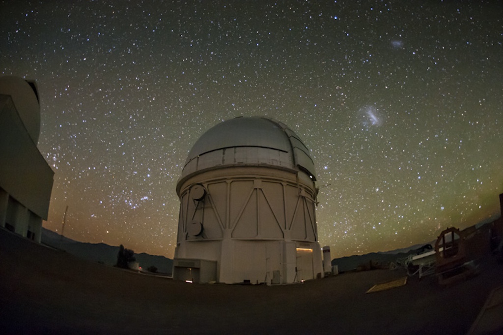
To study dark energy, the DES collaboration carried out a deep, wide-area survey of the sky from 2013 to 2019. Fermilab built an extremely sensitive 570-megapixel digital camera, DECam, and installed it on the U.S. National Science Foundation Víctor M. Blanco 4-meter telescope at NSF Cerro Tololo Inter-American Observatory, a Program of NSF NOIRLab, in the Chilean Andes. For 758 nights over six years, the DES collaboration recorded information from 669 million galaxies that are billions of light-years from Earth, covering an eighth of the sky.
For the latest results, DES scientists greatly advanced methods using weak lensing to robustly reconstruct the distribution of matter in the universe. They did this by measuring the probability of two galaxies being a certain distance apart and the probability that they are also distorted similarly by weak lensing. By reconstructing the matter distribution over 6 billion years of cosmic history, these measurements of weak lensing and galaxy distribution tell scientists how much dark energy and dark matter there is at each moment.
“One of the most exciting parts of the final DES analysis is the advancement in calibrating the data,” said Alexandra Amon, co-lead of the DES weak lensing working group and assistant professor of astrophysics at Princeton University. “The methodologies that our team developed form the bedrock of next-generation surveys.”
In this analysis, DES tested their data against two models of the universe: the currently accepted standard model of cosmology — Lambda cold dark matter (ΛCDM) — in which the dark energy density is constant, and an extended model in which the dark energy density evolves over time — wCDM.
DES found that their data mostly aligned with the standard model of cosmology. Their data also fit the evolving dark energy model, but no better than they fit the standard model.
However, one parameter is still off. Based on measurements of the early universe, both the standard and evolving dark energy models predict how matter in the universe clusters at later times — times probed by surveys like DES. In previous analyses, galaxy clustering was found to be different from what was predicted. When DES added the most recent data, that gap widened, but not yet to the point of certainty that the standard model of cosmology is incorrect. The difference persisted even when DES combined their data with those of other experiments.
“What we are finding is that both the standard model and evolving dark energy model fit the early and late universe observations well, but not perfectly,” said Judit Prat, co-lead of the DES weak lensing working group and the Nordita Fellow at the Stockholm University and the KTH Royal Institute of Technology in Sweden.
Paving the way
Next, DES will combine this work with the most recent constraints from other dark energy experiments to investigate alternative gravity and dark energy models. This analysis is also important because it paves the way for the new NSF-DOE Vera C. Rubin Observatory, funded by the U.S. National Science Foundation and the U.S. Department of Energy’s Office of Science, to do similar work with its Legacy Survey of Space and Time (LSST).
“The measurements will get tighter and tighter in only a few years,” said Anna Porredon, co-lead of the DES Large Scale Structure working group and senior fellow at the Center for Energy, Environmental and Technological Research (CIEMAT) in Madrid. “We have added a significant step in precision, but all these measurements are going to improve much more with new observations from Rubin Observatory and other telescopes. It’s exciting that we will probably have some of the answers about dark energy in the next 10 years.”
More information on the DES collaboration and the funding for this project can be found on the DES website.
The Dark Energy Survey is jointly supported by the U.S. Department of Energy’s Office of Science and the U.S. National Science Foundation.
Fermi National Accelerator Laboratory is America’s premier national laboratory for particle physics and accelerator research. Fermi Forward Discovery Group manages Fermilab for the U.S. Department of Energy Office of Science. Visit Fermilab’s website at www.fnal.gov and follow us on social media.
A lot can happen in the blink of an eye. In a laboratory setting, it takes an average person about one-fifth of a second to see a light and press a button, and in that same interval a hummingbird could beat its wings about a dozen times. Meanwhile, in that same fraction of a second, specialized computer hardware analyzing particle collider data can harness artificial intelligence to make more than 10 million decisions about whether to keep or discard information created by collision events.
“Neural network algorithms help us to gain deeper insights into our data more efficiently to make discoveries much faster than traditional, simple techniques.”
Nhan Tran, head of Fermilab’s AI Coordination Office
At the U.S. Department of Energy’s Fermi National Accelerator Laboratory, researchers are pushing the limits of what machines can do, leading an open-source collaboration to embed neural networks directly into physical hardware in the form of efficient, customized digital circuits. Central to this effort is hls4ml, a software framework developed with Fermilab researchers contributing their expertise. Hls4ml can be used to create ultrafast, decision-making hardware for applications ranging from particle physics to fusion science — and beyond.
Humanity’s most ambitious scientific projects, many led by Fermilab or supported by Fermilab researchers, generate staggering amounts of data. Particle collider detectors, such as CMS at the Large Hadron Collider at CERN, probe the universe at its most fundamental level. Fermilab is the host laboratory in the U.S. that facilitates participation of hundreds of U.S. physicists from more than 50 institutions in the CMS experiment at CERN.
“The CMS upgrades for the High-Luminosity LHC will produce almost six times more data when it starts running in the 2030s,” said Anadi Canepa, a senior scientist at Fermilab and spokesperson for the international CMS collaboration. “Our updated trigger system will allow us to access more granular information, extended coverage and extended timing information. The challenge is that if we analyze all this extra data, we need to do it fast.”
Neural networks — algorithms inspired by the way the human brain processes information — learn by passing data through interconnected layers, adjusting connections to recognize patterns and make predictions. But learning alone isn’t enough; these networks must also be deployed efficiently to deliver real-world value.
“Neural network algorithms help us to gain deeper insights into our data more efficiently to make discoveries much faster than traditional, simple techniques,” said Nhan Tran, head of Fermilab’s AI Coordination Office.
Once a network is modeled and trained, researchers need a clear path to accelerate it in hardware. That’s where hls4ml comes in.
“Hls4ml takes code for neural networks, which can be written with open-source machine learning libraries like PyTorch and TensorFlow, and essentially turns them into a series of logic gates,” Tran explained.
Traditionally, central processing units, commonly called CPUs, and graphics processing units, or GPUs, found in laptops and desktop computers have been used to perform machine learning algorithms.
“As these methods became more widely used, it was natural to ask whether there was a more efficient approach,” said Giuseppe Di Guglielmo, principal engineer at Fermilab.
By moving neural networks onto specialized hardware such as field-programmable gate arrays and application-specific integrated circuits, researchers can perform many calculations at once and make decisions faster while using less power.
“Even though they are more complicated to program, they let us run sophisticated algorithms in real time, where latency and power matter,” Di Guglielmo added.
Programming these devices traditionally requires deep expertise. With hls4ml, however, preparing decision-making hardware for particle detector triggers becomes attainable to a broader range of researchers.
“The hls4ml team is making the trigger more accessible,” said Canepa. “Anyone who has a new idea can now write an algorithm for the trigger and run it. Hls4ml is absolutely critical to the success of the CMS upgrade, because we will collect an unprecedented, very large and complex data set. Without a capable trigger system to select events, we would not be able to store the most interesting collisions.”
“Many fields of cutting-edge science confront big data challenges and explore the nature of the universe at very short timescales, so research communities ranging from fusion energy to neuroscience and materials science are very interested in what we’re doing to enable new capabilities through the power of AI,” added Tran.
Fermi National Accelerator Laboratory is America’s premier national laboratory for particle physics and accelerator research. Fermi Forward Discovery Group manages Fermilab for the U.S. Department of Energy Office of Science. Visit Fermilab’s website at www.fnal.gov and follow us on social media.
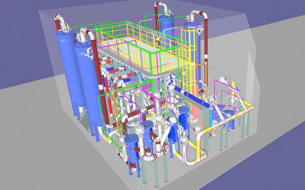
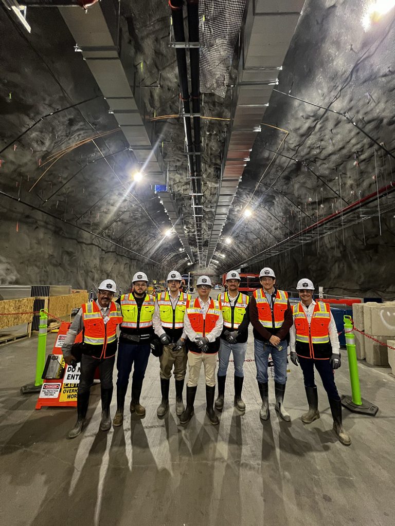
How do you contain over 15,000 tons of a liquid that must be kept at minus 303 degrees Fahrenheit for a science experiment? A science fiction author might send it up to outer space in a fancy tin can since it’s very cold there and everything is weightless. The Deep Underground Neutrino Experiment, a nonfictional experiment with detectors that will be immersed in huge baths of cryogenic liquid argon, is going the opposite direction — down.
“By going underground, the DUNE detectors in South Dakota will significantly reduce cosmic backgrounds.”
Vincent Basque, Fermilab researcher
DUNE is the most sensitive experiment ever conceived for learning about the origins of the universe from the properties of neutrinos, among the first particles to be emitted by the Big Bang. The experiment needs to shield its particle detectors from the cosmic rays that constantly jet through space and bombard the Earth, lest they overwhelm and mask the relatively faint signals the experiment aims to capture. So DUNE researchers will build and run these detectors at the Sanford Underground Research Facility in Lead, South Dakota, underneath a mile of earth that will absorb most of the cosmic traffic.
“By going underground, the DUNE detectors in South Dakota will significantly reduce cosmic backgrounds,” said Fermilab postdoctoral researcher Vincent Basque. “This allows us to study neutrinos sent from the Fermilab beam in Illinois with high precision, detect neutrinos from astrophysical sources like the sun or a nearby supernova, and search for other extremely rare processes.”
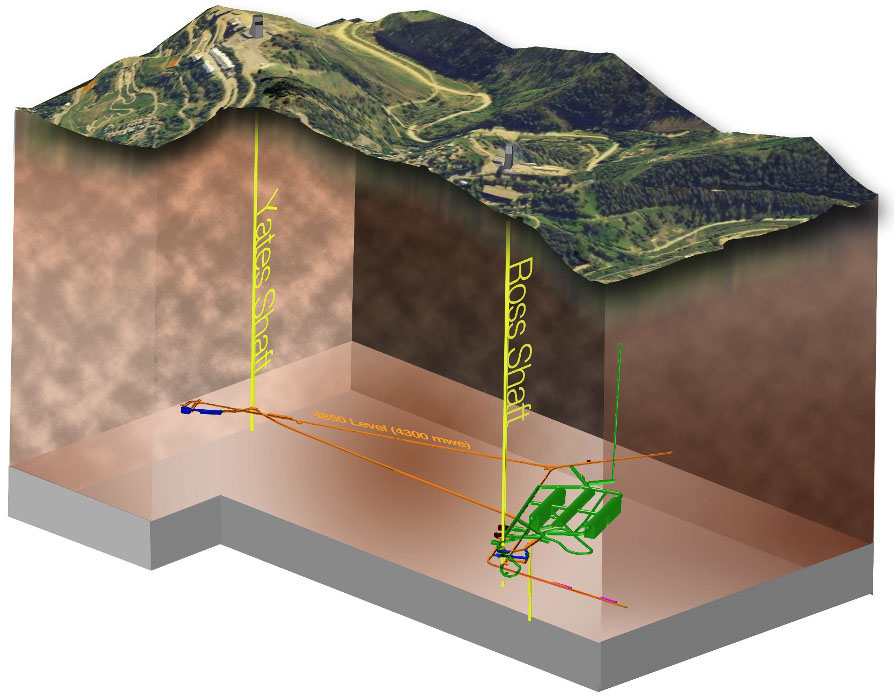
The DUNE collaboration — hosted by the U.S. Department of Energy’s Fermi National Accelerator Laboratory — is currently preparing to install two of these multi-kiloton detector modules using variants of liquid-argon time projection chamber, or LArTPC, technology. International collaborators hope to contribute an additional two modules in coming years. Each module will be housed in an insulating container called a cryostat that is nearly 500,000 cubic feet in size — roughly the same volume as five Olympic-size swimming pools. Far from being available at your local hardware store, CERN has contracted with GTT, a company that designs cryostats for shipping liquefied natural gas, to design the cryostats. GTT has been designing smaller cryostats for CERN experiments since 2007. CERN, the largest European center for nuclear research that is collaborating on DUNE, is contributing the cryostats for the experiment.
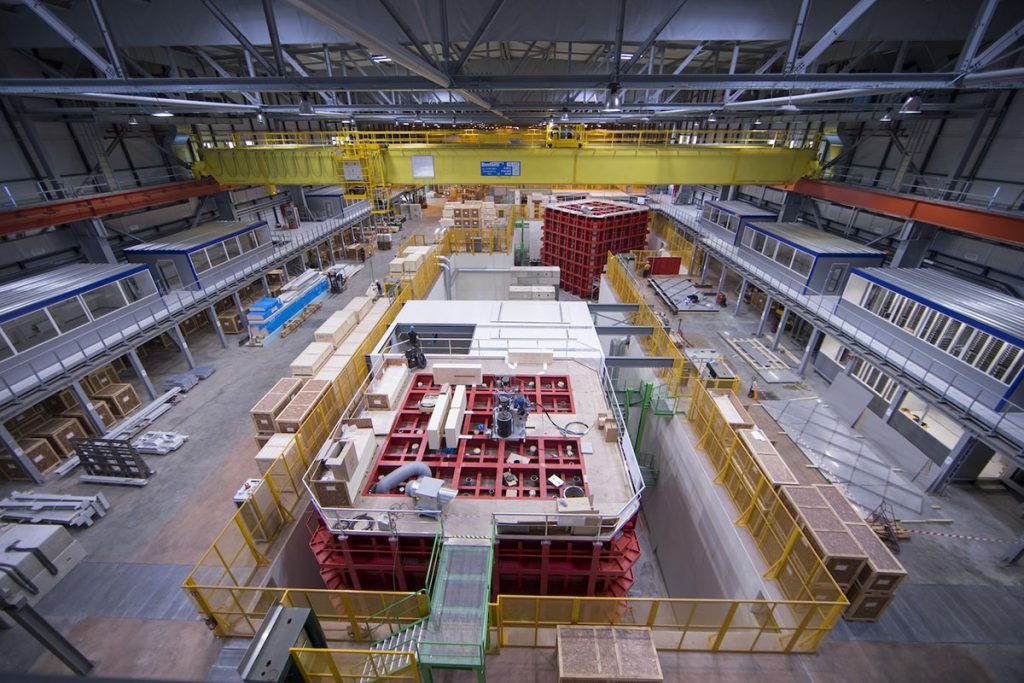
Cryostats for liquid-argon time projection chambers must be robust enough to resist the outward pressure of the fluid (1.4 times denser than water) and pliant enough to retain their integrity over a roughly 375 degrees Fahrenheit range between room and liquid argon temperatures. They must also be sufficiently insulated to maintain the cryogenic temperature level and able to accommodate an industrial-scale cryogenics system to maintain the required argon purity. Beyond that, CERN will construct the cryostats in place from pieces that fit down a 4-by-6-meter mine shaft.
“Making this possible has required detailed and precise design and logistics planning.”
Lluís Miralles Verge, CERN
“It’s the first time we will do something this big,” said Lluís Miralles Verge, the leader for the experiment’s cryostat project at CERN. “The DUNE LArTPCs will be installed in caverns that can only be reached via a deep shaft. Making this possible has required detailed and precise design and logistics planning.”
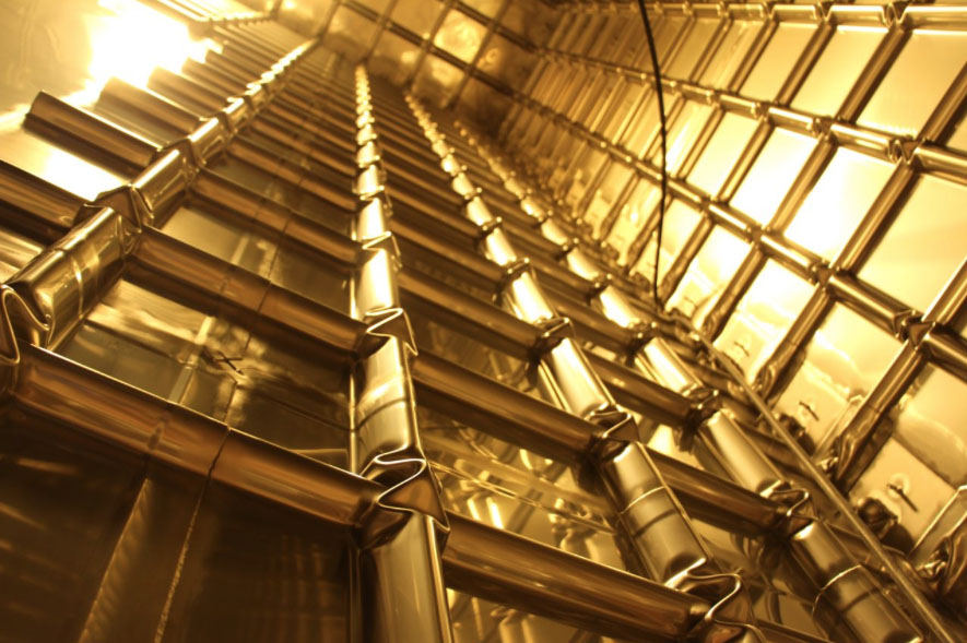
To achieve leakproof liquid and vapor containment, in addition to adequate insulation and support, the DUNE cryostats are composed of several layers. GTT’s tried-and-true design is of a style known as a membrane cryostat, because of the innermost layer that forms a membrane to contain the liquid cryogen. This layer, and all the others, come down the shaft in pieces and are assembled in the detector cavern, starting with the outer structure. Completion of the inner portions of a DUNE cryostat requires more than 5,000 individual pieces.
The primary and innermost layer is constructed of stainless steel, a material that doesn’t exude anything that could contaminate the argon. The corrugated sections are welded together to form the leakproof membrane that is in direct contact with the liquid argon.
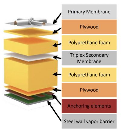
Why the corrugations? They are important for mitigating the contraction effects in both dimensions on the metal as it cools to its final cryogenic temperature. Without them, the cryostat’s length would shrink by an impressive 20 inches or so, and burst the welds. Instead, each corrugation changes shape very slightly and the welds hold. Controlling the membrane contraction also, and importantly, helps keep the detector precisely in position.
“The DUNE prototypes at CERN have been invaluable,” said David Montanari, cryogenics project manager for DUNE. “They have demonstrated that the detector elements, cryostats and cryogenics work together properly, giving us confidence that the DUNE far detector cryostats will perform flawlessly.”
Fermi National Accelerator Laboratory is America’s premier national laboratory for particle physics and accelerator research. Fermi Forward Discovery Group manages Fermilab for the U.S. Department of Energy Office of Science. Visit Fermilab’s website at www.fnal.gov and follow us on social media.