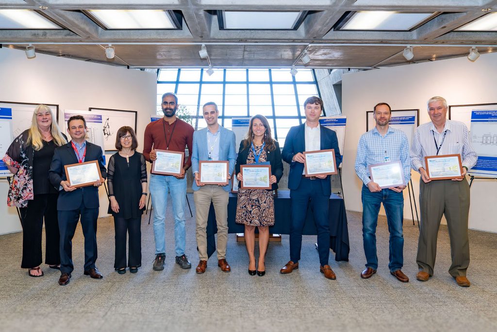
Fermilab feature

QUIET: a place to study qubits shielded from the effects of cosmic rays

Tags:

Deep under the ground at Fermi National Accelerator Laboratory is a brand-new quantum sensor and computing research center called QUIET, and at the surface — 100 meters above — sits its twin called LOUD.

The quantum research infrastructure is among the first of its kind to be operational in the United States. Together, QUIET and LOUD will allow for controlled experiments with quantum sensors to make direct comparisons between an environment with significantly reduced cosmic ray interference and the ambient environment on Earth’s surface.

Quantum information stored in qubits is fragile: Interactions from the environment cause the quantum states to decohere and eventually collapse into a single state. Because superconducting qubits are negatively impacted by cosmic rays and associated energetic particles like muons, understanding how this impacts these delicate devices is crucial. The knowledge gained could enable researchers to better manipulate and protect quantum states and even contribute to a further range of applications, including the detection of dark matter.

The QUIET laboratory is 100 meters below ground at Fermilab. Photo: Ryan Postel, Fermilab

High-energy particles impact superconducting qubits

“It’s not a surprise that when one of these very energetic particles — an X-ray, a gamma ray, or another kind of cosmic ray — hits your qubit, it wipes out all the information,” said Fermilab scientist Aaron Chou, who leads the Quantum Devices and Sensors for Discovery Science thrust of the Quantum Science Center, headquartered at the Department of Energy’s Oak Ridge National Laboratory. Fermilab is a founding partner of the QSC.

The information on a quantum chip can be destroyed within a fraction of a second due to this interference, resulting in the qubits losing information. This will appreciably limit large-scale calculations in quantum computers, according to Fermilab scientist and QSC member Daniel Baxter.

“It isn’t a problem yet, but we will see it in the future,” Baxter said. “The goal is to resolve it before we get there, because we know it’s going to be a limiting factor. If we solve it ahead of time, we will clear the runway for ourselves as we take the path towards quantum computing.”

One goal of QUIET is to understand the difference between the impact of gamma rays, X-rays, muons, and beta particles on superconducting qubits. There are big differences in how those particles interact in a material. For example, a beta particle will interact with the atoms on the surface of a material, while a muon will pass through, depositing energy over a longer distance and deeper into the material. However, little is currently known about the nuances of how those particles interact with superconducting qubits.

Utilizing QUIET to understand the impact of high-energy stray particles on superconducting qubits could allow researchers to construct new models that are less sensitive to radiation. This research involves taking qubits that have been tested at the surface and then moving them underground — where the muon and cosmic ray flux is much smaller — to determine how their performance changes. Potential new models could work one of two ways: researchers could either focus on shielding qubits from the interference, or design devices that are not sensitive to it in the first place.

Dark matter applications

Alternatively, using qubits as sensors for making new detectors that are hypersensitive to radiation could also be useful for the detection of dark matter.

Currently, dark matter detection is limited by most techniques sensitive only above the electron volt scale, which represents the energy gained when an electron charge is accelerated through a potential difference of one volt. These new hypersensitive quantum sensors that could detect below the eV scale may allow scientists to test a wider suite of theoretical models for dark matter.

“A more sensitive detector using superconducting qubits, which can go by a factor of more than a thousand below the eV scale, will allow us to detect energy deposits that are much smaller than what is possible in current dark matter experiments,” Chou said. “This will allow us to detect dark matter of lower mass because it’s easier to detect that you’ve been hit with a freight train than a ping pong ball.”

Deep underground

QUIET was constructed as part of the National Quantum Initiative. The underground space it uses was originally created by Fermilab for its neutrino experiments. Neutrino beamlines are safe to be in when the beams are on, and the space provided can be used for other experiments.

“Underground facilities are quite a rare and unique thing that Fermilab has, and Fermilab is taking advantage of this underground space for cutting-edge science,” Baxter said. The convenience of QUIET is also notable in comparison to other underground spaces. “If I’m sitting in my office, I can be underground in ten minutes,” Baxter added.

Quantum and dark matter scientists around the world are planning similar underground quantum testing facilities in deep mines. For example, scientists with Fermilab’s Superconducting Quantum Materials and Systems Center have started testing qubits in the laboratory built beneath Gran Sasso mountain in Italy. While QUIET is not as deep, it’s accessibility provides a great advantage.

Additionally, other national laboratories have underground spaces. QUIET provides a 99% reduction in muon flux and gives scientists the opportunity to take advantage of this easily accessible underground resource for cutting edge science.  

The underground QUIET laboratory space provides shielding from interference caused by cosmic rays. Photo: Ryan Postel, Fermilab

The Future of QUIET

QUIET — which took two and a half years to build — is currently in its commissioning phase and should be operational in the next few months. Scientists have installed and tested a dilution refrigerator, which is necessary for the deployment of superconducting qubits. They are also setting up radio frequency electronics, which superconducting qubits use to control and read out their quantum states. Many of the individual components of the research space, such as the fridge and electronics, are commercial items that were purchased for both QUIET and LOUD to provide direct one-to-one comparisons.

“It took a significant amount of work behind the scenes to make QUIET’s debut,” said QSC Director Travis Humble. “These efforts included installing dedicated chilled water and electrical power to a newly constructed clean room, among other infrastructure development.”

QUIET and LOUD are funded through the QSC, one of five DOE National Quantum Information Science Research Centers established to support the National Quantum Initiative.

“This is a really exciting and fast-moving field, with new research constantly coming out and changing the discussion, and it’s exciting that Fermilab is one of the main players in such a relevant and high-stakes subject,” Baxter said.

Fermi National Accelerator Laboratory is supported by the Office of Science of the U.S. Department of Energy. The Office of Science is the single largest supporter of basic research in the physical sciences in the United States and is working to address some of the most pressing challenges of our time. For more information, please visit science.energy.gov.

Scientists and engineers at the Superconducting Quantum Materials and Systems Center, hosted by the U.S. Department of Energy’s Fermi National Accelerator Laboratory, have achieved reproducible improvements in superconducting transmon qubit lifetimes with record values of 0.6 milliseconds. The result was achieved through an innovative materials technique that eliminated a major loss source in the devices. 

These results have been published in Nature Partner Journal Quantum Information. 

Quantum devices such as qubits are critical for storing and manipulating quantum information. The qubit lifespan, known as coherence time, determines how long data can be stored and processed before an error occurs. This phenomenon, called quantum decoherence, is a key obstacle to operating quantum processors and sensors.  

Electron microscopy images show the surface of the various superconducting transmon qubits fabricated at SQMS with the novel encapsulation technique. The qubit with the native niobium oxide is compared to the tantalum and gold capping layers that prevent the re-growth of the niobium oxide. Graphic: SQMS Center, Fermilab

The novel process called “surface encapsulation” protects key layers of the qubit during fabrication and prevents the formation of problematic, “lossy” oxides at the surfaces and interfaces of these devices. By carefully investigating and comparing various materials and deposition techniques, SQMS researchers have studied different oxides that lead to longer qubit lifetimes and fewer losses.   

“SQMS is pushing the envelope of qubit performance,” said Alexander Romanenko, a senior scientist at Fermilab and SQMS Center’s quantum technology thrust leader. “These efforts show that undergoing a systematic review of processes and materials and attacking what matters most first is the key to pushing qubit coherence. Pursuing device fabrication and characterization, hand in hand with materials science is the right recipe to deepen our scientific understanding of loss mechanisms and improve quantum devices in the future.”  

Anna Grassellino, Fermilab senior scientist and SQMS Center Director, and Akshay Murthy, SQMS Materials Focus Area Leader and Materials Characterization group leader, apply state-of-the-art characterization techniques in the Materials Science Lab, such as x-ray photoelectron spectroscopy and time-of-flight secondary ion mass spectrometry to examine the effectiveness of niobium surface capping. Photo: Ryan Postel, Fermilab

Anna Grassellino, Fermilab senior scientist and SQMS Center director, and Akshay Murthy, SQMS Materials Focus area leader and Materials Characterization group leader, apply state-of-the-art characterization techniques in the Materials Science Lab, such as X-ray photoelectron spectroscopy and time-of-flight secondary ion mass spectrometry, to examine the effectiveness of niobium surface capping. Photo: Ryan Postel, Fermilab

The biggest hurdle for qubits: coherence time

There are many types of qubits. These basic building blocks of quantum computers process information differently — and potentially faster — than classical computers. The longer a qubit can store quantum information, the better its potential for use in a quantum computer.

Since its inception in 2020, the SQMS research team has focused on understanding the source of errors and decoherence in transmon qubits. This type of qubit is patterned on a chip consisting of a metallic niobium layer on top of a substrate, such as silicon or sapphire. Many consider these superconducting qubits to be the most advanced platform for quantum computers. Tech companies in the United States and around the world are also exploring them.  

Mustafa Bal, nanofabrication group leader at the Fermilab SQMS division and leader of the SQMS Center national nanofabrication taskforce (left) and graduate student Francesco Crisa hold transmon chips of leading performance they produced at the Pritzker Nanofabrication Facility. Photo: Dan Svoboda, Fermilab

However, scientists must still overcome some challenges before quantum computers can fulfill their promise of solving previously unsolvable problems. Specific properties of the materials used to create these qubits can lead to the decoherence of quantum information. At SQMS, developing a deeper scientific understanding of these properties and loss mitigation strategies is an active area of research.  

To make qubits last longer, focus on the materials

Shaojiang Zhu, qubit design and simulation group leader at the Fermilab SQMS Division, holds transmon qubits prepared with the surface encapsulation technique ready to be measured at the SQMS Quantum Garage at Fermilab. Photo: Dan Svoboda, Fermilab

SQMS scientists studying the losses in transmon qubits pointed to the niobium surface as the primary culprit. These qubits are fabricated in a vacuum, but when exposed to air, an oxide forms on the surface of niobium. Though this oxide layer is thin — only about 5 nanometers — it is a major source of energy loss and leads to shorter coherence times. 

Our prior measurements indicate that niobium is the best superconductor for these qubits. While the metal losses are near zero, the niobium surface oxide is problematic and the main driver of losses in these circuits.” Romanenko said.   

SQMS scientists proposed encapsulating the niobium during fabrication so it would never be exposed to air and, therefore, its oxide would not form. While they had a hypothesis on which materials would work best for capping, determining the optimal material required a detailed study. So, they systematically tested this technique with different materials, including aluminum, tantalum, titanium nitride, and gold.   

With each capping layer attempt, SQMS scientists analyzed the materials using several advanced characterization techniques at material science labs at Fermilab, Ames National Laboratory, Northwestern University, and Temple University. Qubit performances were measured inside a dilution refrigerator at the SQMS Quantum Garage at Fermilab. This cryogenic device cools qubits to just a tick above absolute zero. The results demonstrated that the researchers could prepare qubits with 2 to 5 times coherence improvement compared to samples prepared without a capping layer (containing the niobium oxide layer).  

The team found that the capping process improved coherence times for all materials explored in the study. Of these materials, tantalum and gold proved to be the most effective for enabling a higher coherence time, with an average of 0.3 milliseconds and maximum values as high as 0.6 milliseconds. These results shed further light on the nature, hierarchy, and the mechanism of losses in these qubits. They are found to be driven by the presence of amorphous oxides and interfaces.   

“When fabricating a qubit, there are many variables, more or less hidden, that can impact performance,” said Mustafa Bal, a scientist at Fermilab and head of the SQMS nanofabrication group and task force. “This is a first-of-its-kind study that very carefully compares one material change and one process change at a time, on a chip of a fixed geometry, across different fabrication facilities. This approach ensures that we develop reproducible techniques for improvement in qubit performance.”  

Coherence times: how far we have come

The teams fabricated and tested qubits in different facilities as part of the SQMS Center’s National Nanofabrication Taskforce. Fermilab led the way with the SQMS nanofabrication group headed by Bal, making qubits at the Pritzker Nanofabrication Facility at the University of Chicago. Other facilities included Rigetti Computing, a quantum computing company with a quantum foundry, and the National Institute of Standards and Technology Boulder Laboratories. Both are flagship partners at the SQMS Center. Fabricating the chip at Rigetti’s commercial foundry proved that the technique is easily reproducible and scalable for the industry.

“At Rigetti Computing, we want to make the best possible superconducting qubits to make the best possible quantum computers, and extending the lifetimes of qubits in a reproducible way has been one of the hardest problems,” said Andrew Bestwick, senior vice president of quantum systems at Rigetti. “These are among the leading transmon coherence times that the field has been able to achieve on a two-dimensional chip. Most importantly, the study has been guided by the scientific understanding of qubit loss, leading to reproducibility across different labs and in our fabrication facility.”

Rigetti’s Fab-1 is the industry’s first dedicated and integrated quantum device and manufacturing facility, located in Fremont, California. The qubit surface encapsulation technique was easily reproduced at the Rigetti facilities. Photo: Rigetti Computing

At NIST, scientists are interested in using quantum technology to make fundamental measurements of photons, microwave radiation, and voltage. “This has been a great team effort and a good planting of a flag that shows both how far we have come and the challenges that remain to be faced,” said Peter Hopkins, a physicist at NIST who leads the superconductive electronics group and is a lead member of the SQMS Center National Nanofabrication Taskforce 

Following this work, SQMS researchers continue to push qubits’ performance frontier further. The next steps include engineering creative and robust nanofabrication solutions for applying this technique to other transmon qubit surfaces to eliminate all lossy interfaces present in these devices. The underlying substrate upon which these qubits are prepared also represents the next major source of losses. SQMS researchers are already hard at work characterizing and developing better silicon wafers or other lower-loss substrates suitable for quantum applications.   

Moreover, SQMS scientists are working to ensure these advances in the coherence studies can be preserved in more complex chip architectures with several interconnected qubits.   

SQMS Quantum Technology Roadmap

Given the breadth of the SQMS Center collaboration, the Center’s vision and mission are multi-fold. The researchers seek to improve the performance of the building blocks of a quantum computer and apply these innovations in mid-scale prototypes of quantum processors.   

At SQMS, two main superconducting quantum computing platforms are under exploration: 2D transmon qubit chip-based and 3D cavity-based architectures. For the chip-based processors, SQMS researchers work hand in hand with industry partners such as Rigetti to advance performance and scalability of these platforms.   

Currently, SQMS researchers from Fermilab and Rigetti have co-developed a 9-qubit processor incorporating these surface encapsulation advances. The chip is being installed in the SQMS Quantum Garage at Fermilab. Its performance will be evaluated and benchmarked in the upcoming weeks.

This timeline shows the SQMS Center’s development of 2D transmon qubits and 3D cavity-based platforms. Graphic: Samantha Koch, Fermilab

This timeline shows shows a roadmap for the SQMS Center’s development of 2D transmon qubits and 3D cavity-based platforms. Graphic: Samantha Koch, Fermilab

For the 3D cavity-based platforms, Fermilab scientists have been working to integrate these qubits with superconducting radio-frequency cavities. Scientists initially developed these cavities for particle accelerators and Fermilab builds upon decades of experience in making the world’s best SRF cavities, demonstrating photon lifetimes of up to 2 seconds. When combined with transmon qubits, these cavities can also be used as building blocks of quantum computing platforms. Such an approach promises potentially better coherence, scalability and qubit connectivity. To date, Fermilab scientists have achieved up to several milliseconds of coherence in these cavity-qubit combined systems.   

“We know how to make the world’s best cavities, but the success of the 3D platforms under construction at Fermilab also heavily depends on how far we can keep pushing the performance of these transmon qubits used to control and manipulate the quantum states in the cavities,” said Romanenko. “So, it’s kind of two birds with one stone. As we push to advance our transformational 3D technologies, we also work alongside industry to enable important advances in 2D chip-based quantum computing platforms.”

The Superconducting Quantum Materials and Systems Center at Fermilab is supported by the DOE Office of Science.  

The Superconducting Quantum Materials and Systems Center is one of the five U.S. Department of Energy National Quantum Information Science Research Centers. Led by Fermi National Accelerator Laboratory, SQMS is a collaboration of more than 30 partner institutions — national labs, academia and industry — working together to bring transformational advances in the field of quantum information science. The center leverages Fermilab’s expertise in building complex particle accelerators to engineer multiqubit quantum processor platforms based on state-of-the-art qubits and superconducting technologies. Working hand in hand with embedded industry partners, SQMS will build a quantum computer and new quantum sensors at Fermilab, which will open unprecedented computational opportunities. For more information, please visit sqmscenter.fnal.gov.  

Fermi National Accelerator Laboratory is America’s premier national laboratory for particle physics research. A U.S. Department of Energy Office of Science laboratory, Fermilab is located near Chicago, Illinois, and operated under contract by the Fermi Research Alliance LLC. Visit Fermilab’s website at https://www.fnal.gov and follow us on Twitter @Fermilab.  


Representatives of the São Paulo Research Foundation, including Executive Director Carlos Américo Pacheco, Scientific Director Márcio de Castro Silva Filho and General Coordinator of Humanities and Arts Sylvio Canuto, visited the U.S. Department of Energy’s Fermi National Accelerator Laboratory in April to gain an overview of the lab’s scientific portfolio.

The foundation, known as FAPESP, is a state funding agency in São Paulo, Brazil that supports research projects across various scientific disciplines in higher education and research institutions.

The visit commenced with a discussion led by Fermilab Director Lia Merminga along with representatives from the lab’s science and engineering teams. The focus of the talk was Fermilab’s Long-Baseline Neutrino Facility and the Deep Underground Neutrino Experiment. 

Ron Ray, the deputy project director for LBNF/DUNE in the U.S., presented an overview of Fermilab’s flagship experiment. This ambitious project involves directing neutrinos from Fermilab’s campus to detectors situated a mile underground in Lead, South Dakota.

Left to right: Andrew Lathrop of Fermilab presenting to Sylvio Canuto, Carlos Américo Pacheco, and Márcio de Castro Silva Filho of FAPESP inside Fermilab's Integrated Engineering and Research Center. Photo: Dan Svoboda, Fermilab

At the Integrated Engineering Research Center, Andrew Lathrop of Fermilab shows an image of the first cosmic ray muon events in a 450 p.s.i. liquid nitrogen cooled 16 Skipper CCD to (left to right) Sylvio Canuto, Carlos Américo Pacheco, and Márcio de Castro Silva Filho of FAPESP. Photo: Dan Svoboda, Fermilab

To gain insight into Fermilab’s neutrino research, the group toured the Integrated Engineering Research Center accompanied by David Montanari, far detector cryogenics manager for LBNF/DUNE U.S. They met with Andrew Lathrop, a senior technical specialist, to view a Skipper CCD, known for its unprecedented sensitivity to weak electrical signals. This technology can help study rare neutrino interactions and potentially provide insights into dark matter.   

Jennifer Raaf, Fermilab’s head of the neutrino division, showcased the new lab space in the IERC dedicated to assembling and testing modules produced in Switzerland for the DUNE ND-LAr near detector. This detector is crucial for DUNE’s physics sensitivity.   

Left to right: Dante Totani and Jennifer Raaf of Fermilab discuss neutrino detector technologies with Sylvio Canuto, Carlos Américo Pacheco, and Márcio de Castro Silva Filho. Photo: Dan Svoboda, Fermilab

Dante Totani, a postdoctoral researcher from the University of California Santa Barbara, works in this lab space to develop X-Arapuca photodetector cold electronics for DUNE. As neutrinos from Fermilab’s accelerator complex interact with argon nuclei, charged particles are produced. The X-Arapuca detectors collect scintillation light generated during this process to help reconstruct neutrino-argon collisions. This system, developed by Brazilian researchers, is a key feature of the DUNE far detector.   

Saravan Chandrasekaran, in-kind contribution coordinator for the Proton Improvement Plan-II accelerator project, led the next segment of the tour. Chandrasekaran highlighted Fermilab’s research and development in accelerator technology — including PIP-II, the particle accelerator designed to provide the world’s most intense beam of neutrinos for the LBNF/DUNE experiment.  

Fermilab researchers develop electromagnets and superconducting cavities using materials like niobium-tin, which lose electrical resistance when cooled. Fermilab will contribute 16 of these ultra-strong magnets to the High-Luminosity Large Hadron Collider Upgrade Project at CERN. 

Giorgio Apollinari, project manager for the HL-LHC upgrade, and Maria Baldini, a scientist, discussed the project’s scope with the group, emphasizing the magnets’ increased current capacity for creating powerful magnetic fields in the LHC upgrade. 

The representatives then learned about Fermilab’s quantum computing research at the Superconducting Quantum Materials and Systems Center, exploring how superconducting cavities, used in accelerators, might serve as quantum computing devices by storing photons briefly. The SQMS Center is one of five National Quantum Information Science Research Centers established by Congress in 2018.

FAPESP representatives stand with members of the Fermilab scientific and engineering staff at the Short Baseline Near Detector. Photo: Dan Svoboda, Fermilab

The tour ended at the Short Baseline Near Detector at Fermilab. Roza Doubnik, a senior cryogenic engineer and technical liaison with Brazil on the LBNF/DUNE project, highlighted SBND’s role as one of Fermilab’s three liquid argon neutrino detectors for the program and its prototyping connection to the LBNF/DUNE cryostats.  

Ornella Palamara, co-spokesperson for SBND, detailed that the detector will capture over a million neutrino-argon interactions yearly using Liquid Argon Time Projection Chamber technology and the X-Arapuca photon light system, similar to DUNE.

Fermi National Accelerator Laboratory is supported by the Office of Science of the U.S. Department of Energy. The Office of Science is the single largest supporter of basic research in the physical sciences in the United States and is working to address some of the most pressing challenges of our time. For more information, please visit science.energy.gov.