Building a state-of-the-art superconducting radio-frequency particle accelerator is a study in precision. Every component must go together exactly right, because the smallest flaw in assembly can compromise how the machine performs for years to come.
An SRF accelerator is made up of a series of thermos-like vessels called cryomodules that insulate metal accelerating structures, called cavities. These cavities enable the technology’s super-efficient particle acceleration, but only if their interiors are pristine and their components are installed with exacting accuracy. Misalignment or contamination can degrade performance. In fact, the interiors of these cavities must be spotless, as the tiniest particulates can degrade accelerating efficiency or, worse, render a cavity unusable.
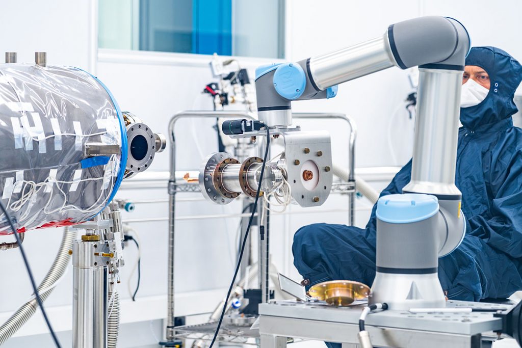
The technicians at the U.S. Department of Energy’s Fermi National Accelerator Laboratory are experts at this rigorous work. They assemble SRF cavities in a “clean room,” taking precautions by wearing protective gear that covers their head, clothing and shoes, along with a mask to filter their breath. But even with these measures, there is significant risk of contaminating the equipment and components.
So, the team behind the Proton Improvement Plan-II project at Fermilab decided to incorporate robots to assist humans assembling accelerator parts inside clean rooms. PIP-II is enhancing the Fermilab Accelerator Complex by building a 215-meter-long linear particle accelerator. The linac will produce high-power proton beams to support new physics experiments at Fermilab and will be used to generate the world’s most powerful neutrino beam for the Deep Underground Neutrino Experiment at the Long-Baseline Neutrino Facility, currently under construction in Lead, South Dakota, and at Fermilab.
“This breakthrough for the SRF community was only possible because of the team’s multidisciplinary composition and effective collaboration.”
Cristian Boffo, PIP-II project director
To enhance precision and maintain an ultra-clean environment during assembly of SRF cavities, the PIP-II team brought in a collaborative robot, known as a “cobot,” in 2023. Unlike a standard industrial robot, a cobot is designed to work safely alongside people and react to contact in its environment. Where an industrial robot is programmed to carry out its task to completion no matter what and is kept in a cage for safety, a cobot is equipped with sensors that allow it to stop or respond if it feels unexpected pressure from bumping into something or someone.
This summer, after three years of development, the PIP-II team reached a major milestone: a cobot autonomously aligned a coupler on an SRF cavity in a clean room. A prime example of Fermilab’s commitment to driving technological innovation, this key step forward in SRF cleanroom assembly allows the cobot to next be deployed on a production cavity for PIP-II.
“This breakthrough for the SRF community was only possible because of the team’s multidisciplinary composition and effective collaboration,” said Cristian Boffo, PIP-II project director.
Precision in a clean room
The PIP-II linac will be made of 23 accelerating units — called cryomodules, because they supply the required liquid helium bath and insulate the cavities from the too-warm outside world, much like a Thermos. PIP-II uses five different types of cryomodule, two of which are called single-spoke resonators: SSR1 and SSR2.
SSR cavities look like very squat soda cans as big as a car tire, and they have a flange on the side for connecting a component called the coupler. Typically, cavities are assembled with two people working inside the clean room, ideally standing at least six feet away from the cavity to limit contamination. In 2016 and 2017, PIP-II technicians tried manually aligning and installing the coupler using prototypes. However, the pieces were heavy and awkward to lift, the angle of connection was unwieldy, and the tooling was too complex.
That’s where the idea arose to utilize a cobot. The PIP-II team needed cobotic help to align and install the coupler with the 16 bolt holes on the flange while minimizing the possibility of human contamination. This task requires submillimeter and subdegree precision — all before the coupler touches the sealing surface. As soon as the cavity is closed, the risk of contamination is gone, and human technicians can re-enter the process.
“We want to bring the technicians as far away from the cavity as possible while the cavity is open — not to replace human technicians,” said Mattia Parise, Fermilab senior engineer and the level-3 manager for the SSR cryomodules for PIP-II.
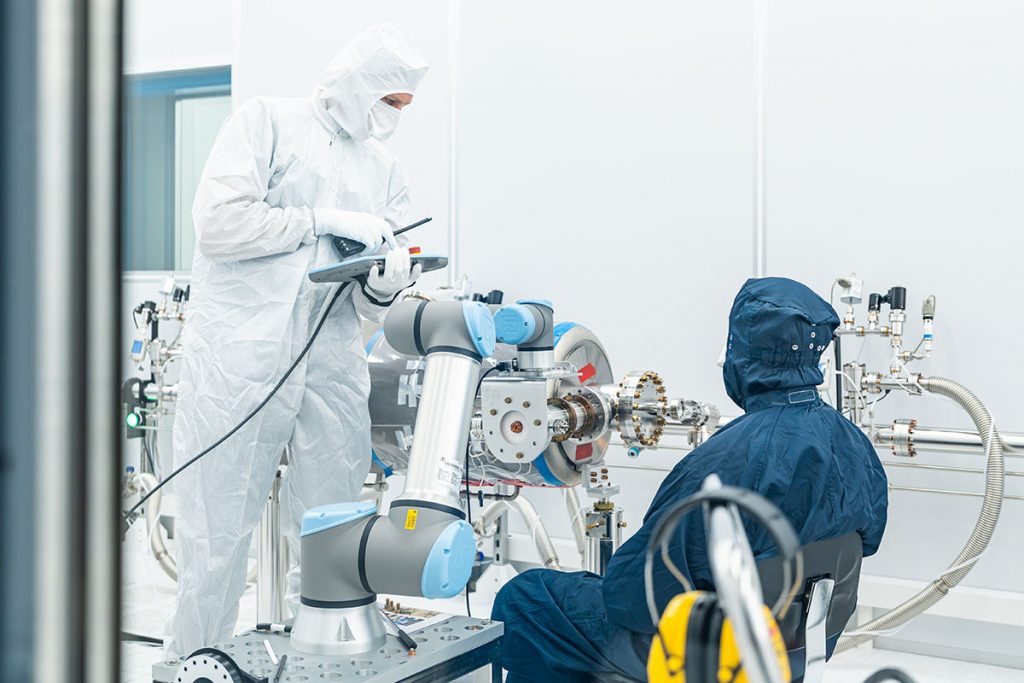
In December 2023, the PIP-II team acquired a cobotic arm with three joints — shoulder, elbow and wrist — that could be controlled by a human outside a clean room. Soon, they had successfully performed their first cobotic installation of a coupler on an SSR2 cavity. PIP-II then procured two additional cobots to boost research and development; over the following three years, they worked with several students from the University of Pisa in Italy and Northern Illinois University in the United States to develop alignment and assembly techniques.
The other piece of the puzzle was to automate the installation. “The goal was always to have this specific part of the process fully automated,” said Parise. “If it’s still semi-automatic and requires the operator to push buttons, you can still make mistakes because you rely on your senses and you’re trying to do alignment with submillimeter precision.”
To automate the coupling process, the PIP-II team added a camera to the cobotic arm. Once calibrated, the camera allowed the cobot to detect the flange’s central hole, align the coupler with the boreholes and connect them together.
In July 2026, they successfully performed the entire process automatically, achieving their three-year-old goal and paving the way for more automated assembly for PIP-II soon.
“Achieving autonomous coupler alignment was a critical first step,” said Tommaso Aiazzi, staff engineer and level-4 and subproject manager for the couplers for PIP-II.
Cobots in the future
All around the world, laboratories are developing robotic or cobotic applications to assemble accelerators or automate clean room processes. “What we are doing differently from everybody else is that we are not relying on plug-and-play solutions,” said Parise.
The problem with off-the-shelf products is that the software usually isn’t scalable or has other limitations because it was developed with a specific application in mind. “Here, we are developing everything from scratch,” said Parise. “We own our process, so we can easily change it because we developed this processing code with our needs in mind.”
This means they have complete adaptability for specialized accelerator applications that can also be tailored to any other existing process that would benefit from automation in a clean room — like the nanofabrication of microchips.
“Whatever application would benefit from automation, we are ready.”
Mattia Parise, senior engineer
The cobot is already speeding up other aspects of assembly, cutting some two- to three-hour cleaning and parts swapping steps down to about an hour. The team is now working to automate a swapping mechanism that currently takes 30 minutes down to as little as 5 seconds.
“There are many ways to improve things with cobotic automation,” said Colin Narug, a staff engineer at Fermilab who has led R&D on the cobotic activities since 2023. “This can cut away some of the more stressful points to make the clean room technicians’ lives easier — and produce better cavity results.”
In 2025, the team connected multiple SSR2 cavities together in a “string” — mostly using cobots. “It was not fully automatic, but we still benefited from this technology and this process,” said Parise.
The team is excited to implement automated cobotic alignment for an SSR1 string assembly this fall. “Whatever application would benefit from automation, we are ready,” said Parise. “Let’s go.”
Fermi National Accelerator Laboratory is America’s national laboratory for particle physics and accelerator research. Fermi Forward Discovery Group manages Fermilab for the U.S. Department of Energy Office of Science. Visit Fermilab’s website at www.fnal.gov and follow us on social media.
I still remember clearly when, six and a half years ago, a few of us sketched the first SQMS logo on a board in a Fermilab hallway.
We knew it had to fit within the shape of a superconducting radio-frequency cavity, a technology that has been at the heart of Fermilab for decades. The name needed to reflect what we believed from the beginning: that better quantum systems require a fundamental understanding of how superconducting materials influence qubit performance, and that an important challenge would be putting everything together at scale. And, of course, it needed a “Q!”
At that moment, SQMS was little more than a name, a logo and an idea on a board.
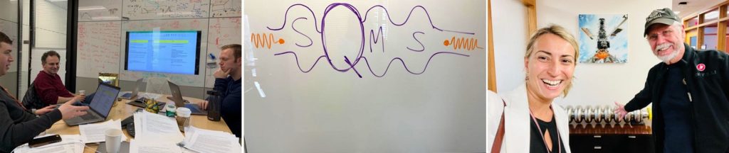
I still find it extraordinary to think about what that sketch has become. Six years ago, that idea became a center, and the center became a community of hundreds of people across the United States and around the world. Together, they have built new experimental capabilities, connected scientific disciplines and trained a new generation of scientists and engineers.
That transformation did not happen because we set out simply to build a larger quantum research program. From the beginning, SQMS was built around a scientific question: What really limits the performance of quantum systems, and how far could we push them if we understood those limits from first principles — the foundational laws of physics?
The origins of that question went back to something Fermilab knew extremely well. Decades of work on superconducting radio-frequency cavities for particle accelerators — structures capable of storing electromagnetic energy with extraordinarily low losses — have produced exceptional expertise in superconducting materials, surfaces, fabrication and processing. Looking at those technologies through the lens of quantum information science revealed that they could preserve quantum information for dramatically longer than many conventional quantum devices.
That observation opened a door. What if the remarkable coherence — the ability to preserve a fragile quantum state — of these three-dimensional superconducting cavities could become the basis for a new kind of quantum architecture? What if the materials science techniques developed to understand accelerator cavities could be applied to the microscopic defects limiting qubits? And what if, instead of treating materials, devices, cryogenics, controls, algorithms and applications as separate problems, we assembled the people who understood each piece and asked them to solve the entire problem together?
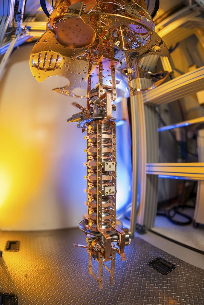
That became the foundation of SQMS. When the Department of Energy selected SQMS as one of its five National Quantum Information Science Research Centers in August 2020, we suddenly had the opportunity — and the responsibility — to turn that idea into something real.
What followed has been one of the most rewarding scientific experiences of my life.
We built SQMS deliberately as a multi-institutional center that unites expertise from laboratories, universities, companies and multiple disciplines. National laboratories brought unique facilities and engineering capabilities; universities contributed deep scientific knowledge and generations of students; and industry brought fabrication, systems know-how, and the perspective needed to translate discoveries into scalable platforms.
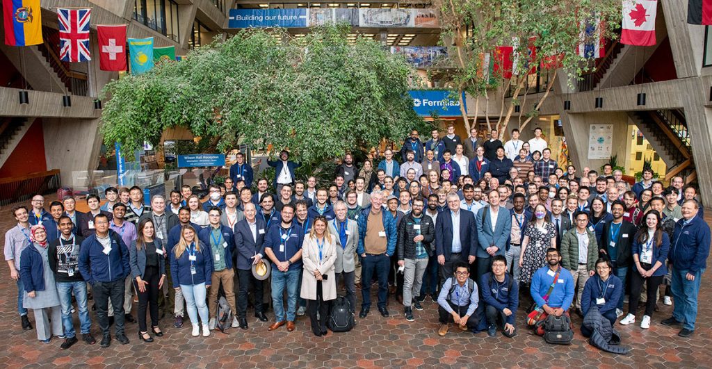
And something important happened in those interactions: people did not simply contribute the expertise they already had. They developed new expertise together. We can see that the original idea worked: when we organize around a sufficiently ambitious scientific challenge, the boundaries between disciplines and institutions become less important than the capabilities each person brings to solving it.
From atoms and interfaces to quantum coherence
One of our starting questions was deceptively simple: Why does a quantum device lose its information?
Quantum information is extraordinarily fragile. Tiny disturbances in a material, microscopic defects at an interface, radiation, magnetic fields or imperfections introduced during fabrication can all create pathways through which quantum information disappears. We call this decoherence, and overcoming it remains one of the central challenges to building useful quantum technologies.
Fermilab brought an unusual perspective to this problem. Years of work on superconducting radio-frequency cavities for particle accelerators had produced cavities capable of storing electromagnetic energy with extraordinarily low losses. Before SQMS formally began, researchers demonstrated microwave photon lifetimes approaching two seconds in these cavity structures — an extraordinary level of coherence that helped inspire the center’s scientific premise.
This work laid the foundations for SQMS to also understand why some superconducting materials and devices perform the way they do, why apparently identical ones sometimes perform differently, and whether that understanding could ultimately allow us to engineer coherence rather than discover it by chance.
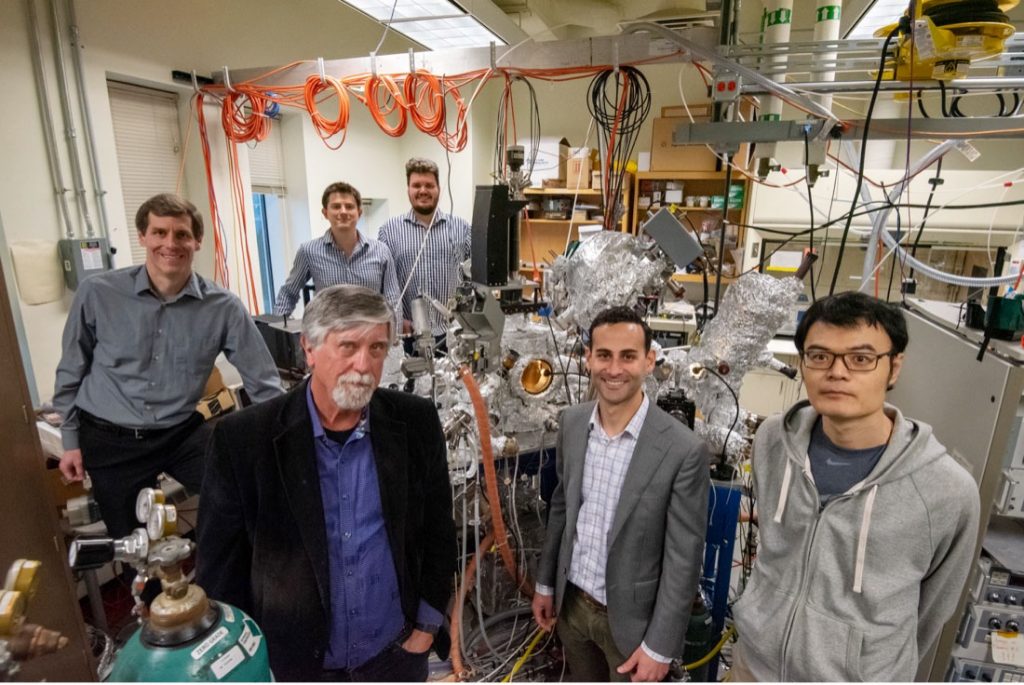
That question brought together people who previously spoke very different scientific languages: quantum-device physicists, materials scientists, chemists, accelerator scientists, microscopists, theorists and engineers. Together, they have progressively peeled back the layers of superconducting quantum devices.
For example, SQMS researchers connected microwave losses in niobium to the microscopic structure and chemistry of its surface oxides, identifying specific defects and mechanisms that can absorb energy from a quantum system. The center investigated why different superconducting qubit materials behave differently, including detailed studies of the structure and formation mechanisms of tantalum and niobium oxides and interfaces, and work explaining why the native oxide of tantalum can suppress magnetic defects and loss mechanisms that are more prevalent in niobium oxide.
Researchers discovered the formation of new defects, such as niobium hydrides, in qubits, which affect performance. And increasingly, SQMS has been able to connect microscopic materials properties directly to the performance spread of actual quantum devices — including understanding why devices fabricated in nominally the same way can nevertheless perform differently.
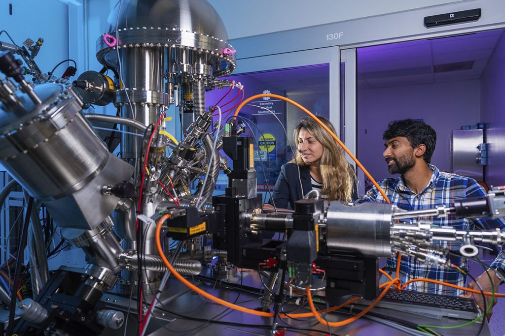
Importantly, this understanding has increasingly translated into methods for actively engineering better, more robust quantum devices. SQMS researchers showed that preventing the formation of lossy niobium surface oxides through surface encapsulation could systematically improve transmon qubit coherence, demonstrating that insights gained from materials science could be translated directly into improved quantum hardware. Transmon qubits are a specific type of superconducting qubit, engineered to be far less sensitive to the small fluctuations in electric charge that can disturb a qubit’s state, making it one of the most widely used qubit designs in superconducting quantum computing today. Today, SQMS routinely fabricates transmon qubit devices with coherence times in the hundreds of microseconds, with some exceeding a millisecond, well beyond the then state-of-the-art 50-100 microsecond values that our partners were observing prior to the center’s inception.
At the same time, researchers have looked beyond the material itself to understand how the surrounding environment affects coherence. Researchers have investigated additional mechanisms that can limit superconducting quantum devices, including magnetic flux trapped inside superconductors as they cool.
Experiments comparing the same superconducting qubit above ground at Fermilab and deep underground at INFN Gran Sasso National Laboratory helped researchers separate the effects of environmental radiation, such as cosmic rays, from sources of noise within the device itself. The results showed that this intrinsic noise still has the greatest effect on overall qubit performance, but radiation can cause brief, identifiable errors that become more important as qubits improve.
SQMS researchers also found that magnetic fields, typically considered harmful to superconducting qubits, can make quantum devices more stable under carefully controlled conditions. This benefit was particularly evident in niobium devices that were surface encapsulated with tantalum metal. In these devices, applying a carefully controlled magnetic flux led to more stable qubit lifetimes without sacrificing long coherence times.
Perhaps the most tangible measure of this progress is not a single record device, but how much the entire collaboration has moved forward together. Early in SQMS, we created the first national Nanofabrication Taskforce, and launched the Round Robin experiment, the first international exchange in which identical qubit chips were measured across different laboratories to systematically expose differences in fabrication, packaging, test setups, controls and measurement protocols. The philosophy was simple: share everything, compare everything and improve together. That approach has helped turn isolated know-how into shared capability, contributing to substantial gains in coherence and reproducibility across the collaboration. SQMS-developed techniques such as surface encapsulation have also been adopted and are now used in laboratories around the world to improve qubit coherence.
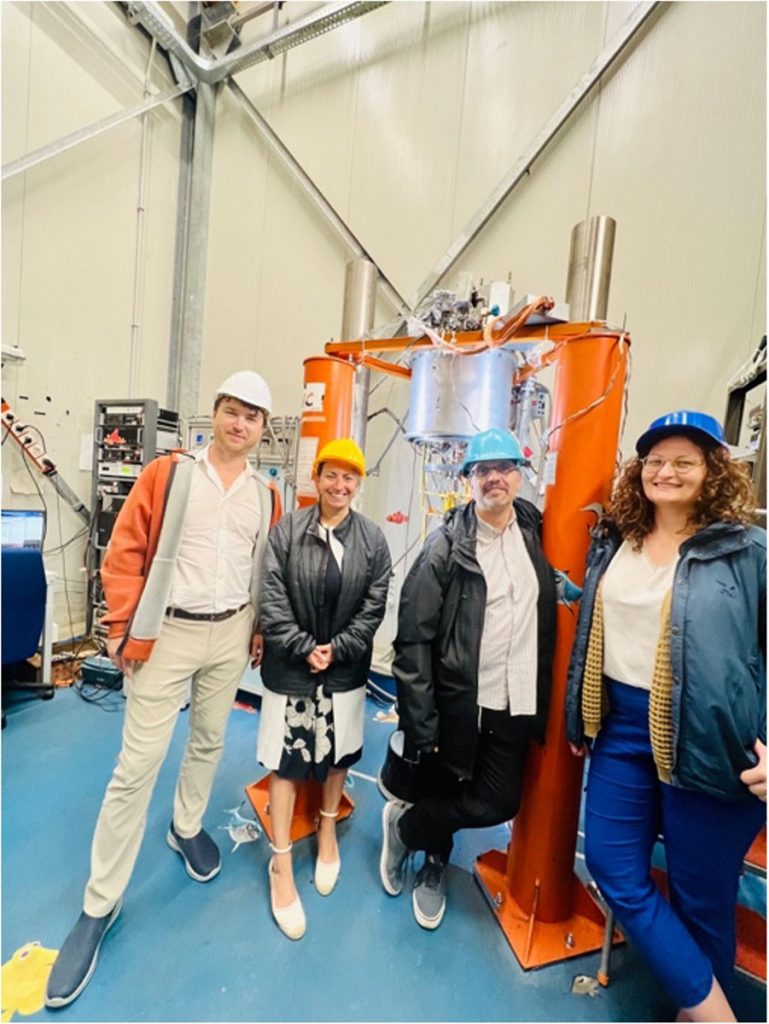
Together, these results show how the SQMS materials program has evolved from identifying sources of decoherence to learning how to control the material, the device and its environment to deliberately improve quantum performance. This progression matters enormously. A future quantum computer cannot depend on finding a few exceptional devices among thousands. Scaling requires reproducibility. We need to understand why one device lives longer than another, which fabrication steps introduce variability, and eventually how to manufacture quantum hardware whose performance can be predicted and controlled.
To me, this represents an important evolution of the field: moving from observing quantum coherence, to understanding it, and ultimately toward engineering it.
From extraordinary coherence to new quantum systems
But understanding coherence was never the final objective. The next question was: What becomes possible if we can preserve quantum information for much longer? Here, one of the technologies that helped inspire SQMS has evolved into something entirely new.
Instead of storing quantum information only in conventional two-level qubits, SQMS has been developing architectures that use the many quantum states available inside ultra-coherent three-dimensional superconducting cavities. These higher-dimensional quantum systems — qudits — can encode and manipulate quantum information in ways that go far beyond qubits.
We have learned how to couple cavities to superconducting control devices, manipulate increasingly complex quantum states and connect these elements into larger systems. Recent demonstrations have brought multiple ultra-coherent cavity modes together with superconducting controls while preserving long coherence, an important step toward programmable cavity-based quantum processors. Other work has developed architectures and techniques for controlling and scaling superconducting quantum systems.
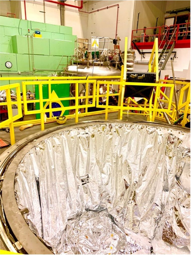
Scaling quantum computing is not simply a matter of making more qubits or qudits. It requires hardware, cryogenics, controls, software and algorithms to operate as one system. SQMS has therefore also worked on the less visible, but essential, technologies of scale, including methods for transferring quantum information between physically separated quantum modules and for efficiently cooling large-scale systems.
This is a transition I find particularly exciting: we are moving from asking, “Can we make an extraordinary quantum device?” to asking,“Can we build an extraordinary quantum system?”
Quantum technologies becoming instruments for discovery
At the same time, technologies developed for quantum science began to find a natural second role in a particle physics laboratory as powerful new instruments for fundamental physics.
A cavity capable of preserving a single microwave photon for an extraordinarily long time is not only a quantum memory. It is also an exquisitely sensitive detector – potentially capable of detecting the incredibly faint signatures of particles left over from the early universe. And quantum processors themselves can become part of physics experiments.
The DarkSRF experiment, for example, repurposed superconducting accelerator cavities as detectors in a search for dark photons — hypothetical particles that could also be a dark matter candidate. The experiment established world-leading laboratory constraints over part of the dark-photon parameter space, offering new clarity on where these dark photons may or may not exist in terms of their mass and interactions with the electromagnetic sector. SQMS researchers are also adapting single-microwave-photon detection techniques to searches for new particles whose signals would otherwise be buried beneath conventional measurement noise.
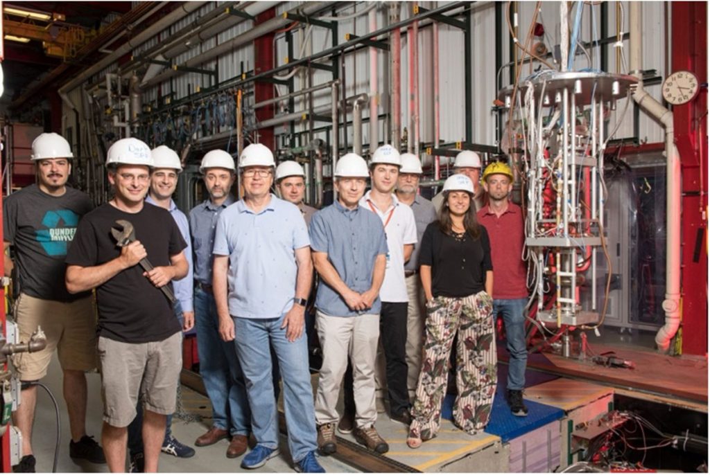
This broader convergence of quantum technology and fundamental physics has also opened new approaches to precision measurements and tests of nature. Perhaps my favorite illustration is an experiment that asked an almost audacious question: Is quantum mechanics itself exactly correct?
Researchers used truly random quantum measurements generated by a superconducting quantum processor in a superbly sensitive cryogenic radio-frequency experiment searching for tiny nonlinear deviations from quantum mechanics. No deviation was found, but the experiment established substantially stronger constraints on how large such an effect could be. Other SQMS work is exploring how quantum technologies can test fundamental principles and probe new regimes of physics.
There is something beautiful about that scientific circle: we built quantum technologies by learning how quantum mechanics works and then used those technologies to test quantum mechanics itself. That is the kind of unexpected scientific connection that becomes possible when technology and fundamental science develop together.
Learning how to compute differently
The hardware has also forced us to think differently about computation itself. Much of today’s quantum computing language was developed around the idea of the qubit — a quantum object with two basic states, analogous to the zero and one of classical computing. But SQMS’s cavity-qudit architecture provides access to many quantum levels within a single physical system.
That means we cannot simply take algorithms and error-correction techniques designed for qubits and assume they are the best way to use this hardware.
SQMS researchers have therefore been developing new ways to control higher-dimensional quantum systems, compile quantum operations and suppress errors. Recent work, for example, developed a precise, repeatable way to translate any operation on a qutrit, a three-level quantum system, into the physical steps needed to run it, an important building block for computation using higher-dimensional hardware.
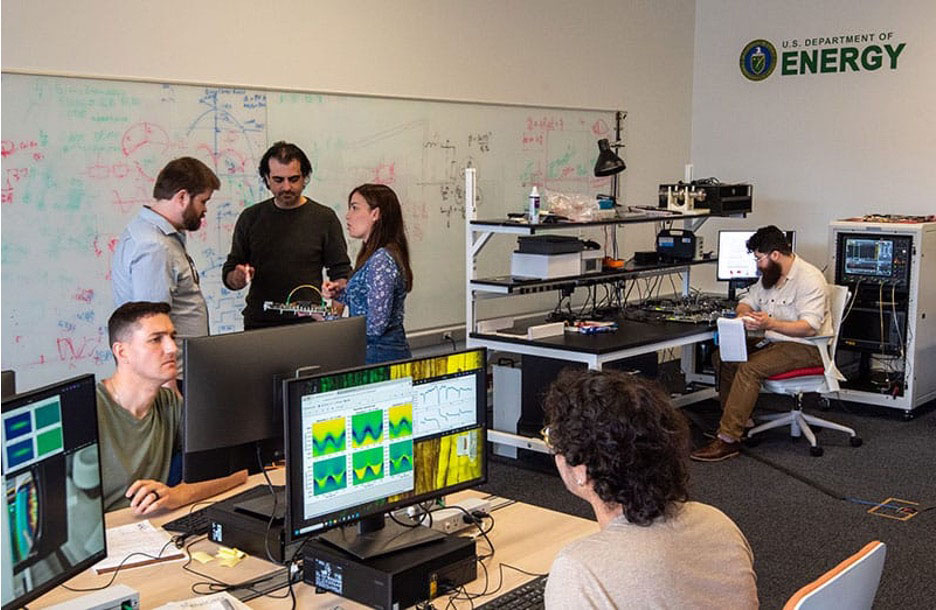
This co-design between hardware and algorithms is essential. Rather than building a machine first and then asking scientists what to do with it later, the hardware architecture, control system, error-correction strategy, algorithms and eventual scientific applications need to inform one another from the beginning.
From better devices to new science
When I put all of this together, what stands out is how interconnected the work has become.
We started by asking why quantum information disappears, a question that took us down to atoms, oxides, interfaces and defects.
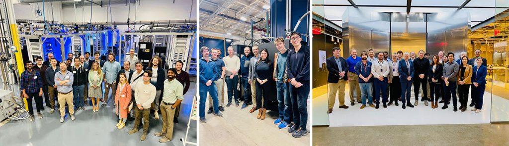
The challenge in front of us is no longer how far we can push an individual quantum device. It is how rapidly we can bring these technologies together into scaled, integrated and accessible quantum platforms capable of doing science. That raises a larger question: What infrastructure will scientists need to make that possible?
In many ways, SQMS has spent its first six years building pieces of the answer.
Building more than technology: people, places and a quantum ecosystem
Scientific ideas ultimately need somewhere to become real. Building on DOE investments across SQMS and its partner network, we set out to create the specialized environments needed for cutting-edge quantum research. As the science of SQMS grew, so did the places where that science could happen.
At Fermilab, spaces that had never housed scientific experiments became some of the most advanced quantum laboratories in the country. The Quantum Garage, once quite literally a garage, is today a 6,000-square-foot quantum laboratory containing six extra-large Bluefors dilution refrigerators and SQMS-developed experimental platforms for quantum computing, sensing, metrology and communications. Built collaboratively, it now supports more than 60 experiments running in parallel.
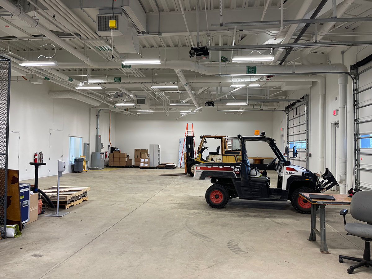
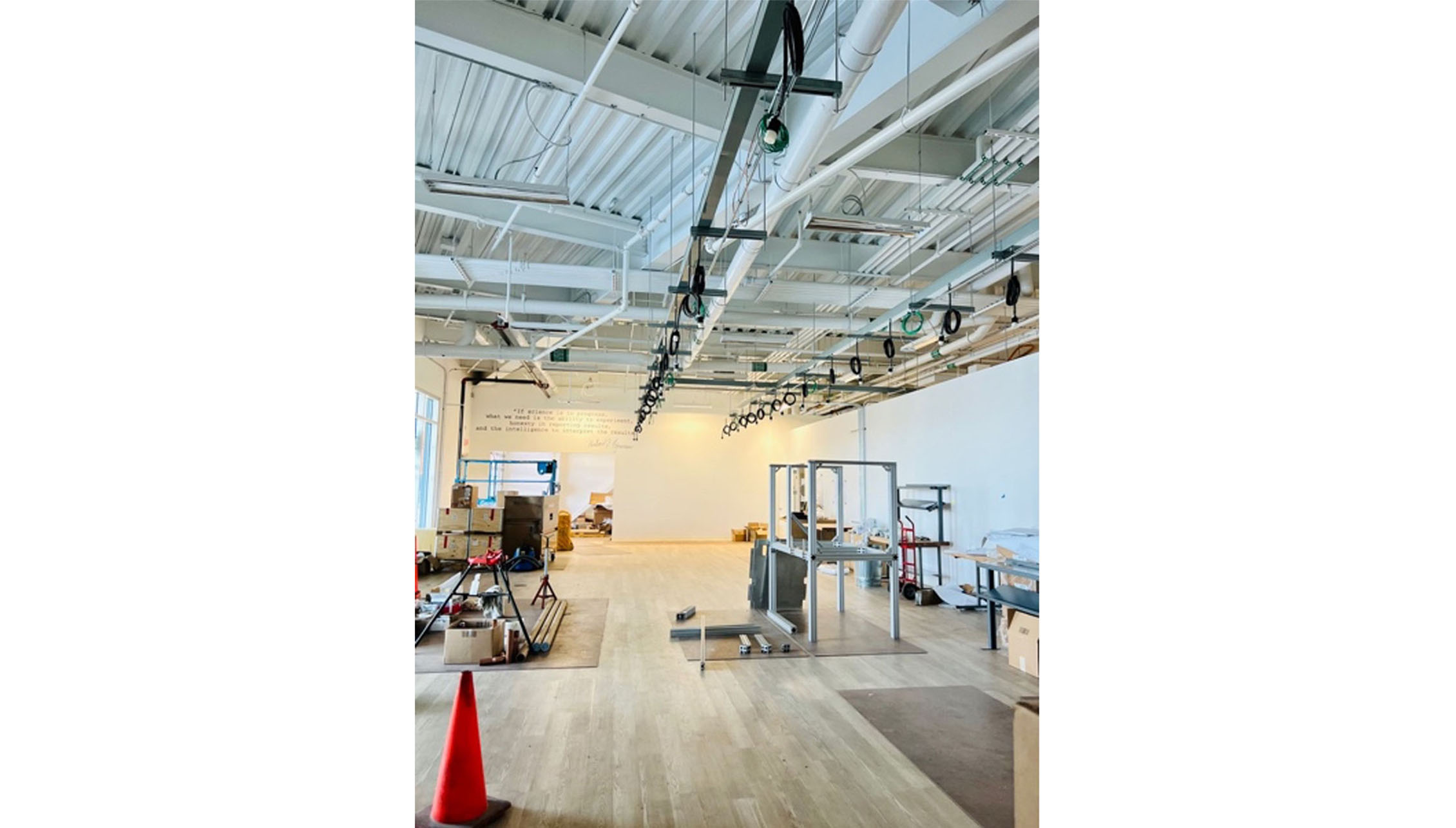
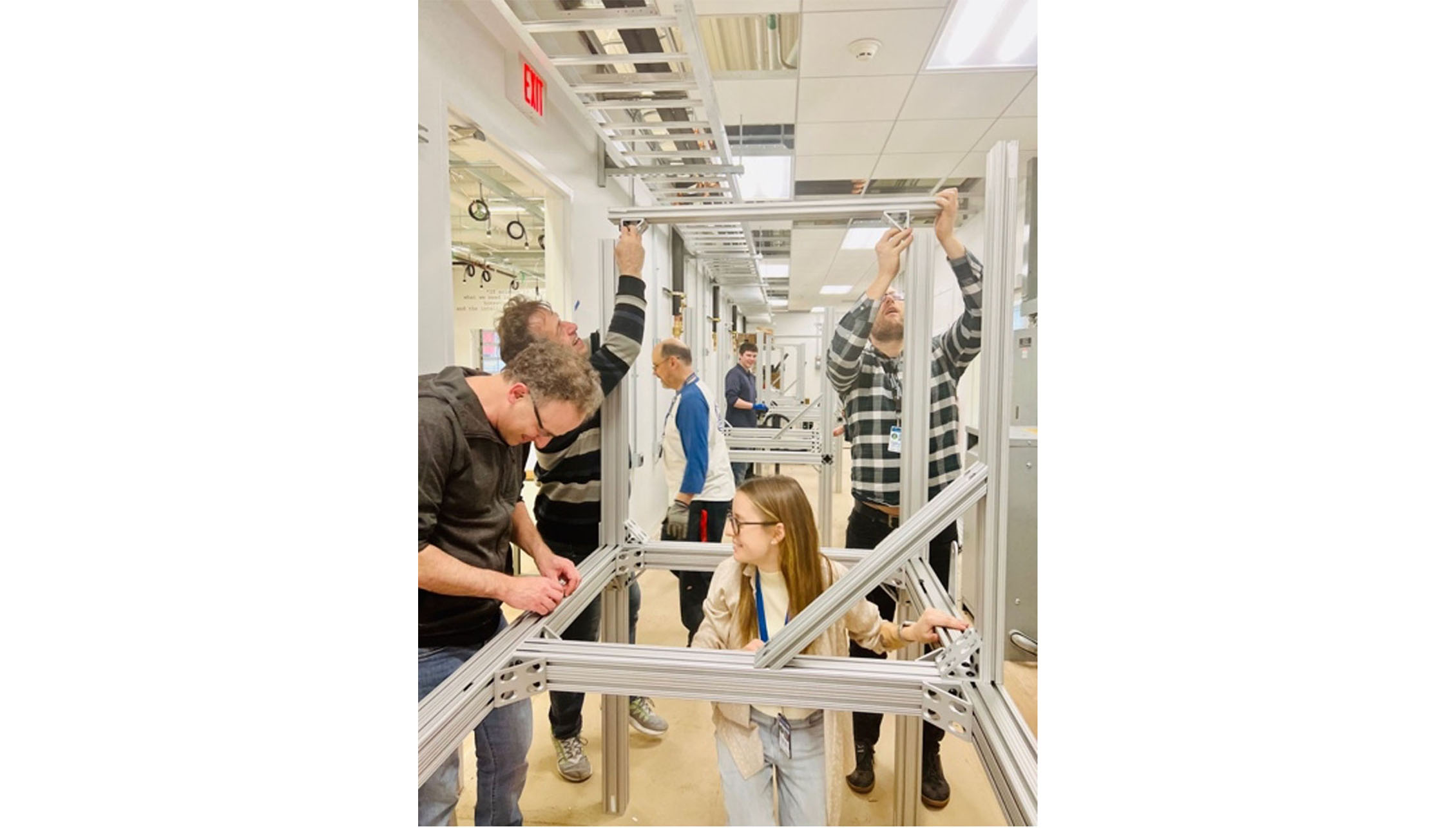
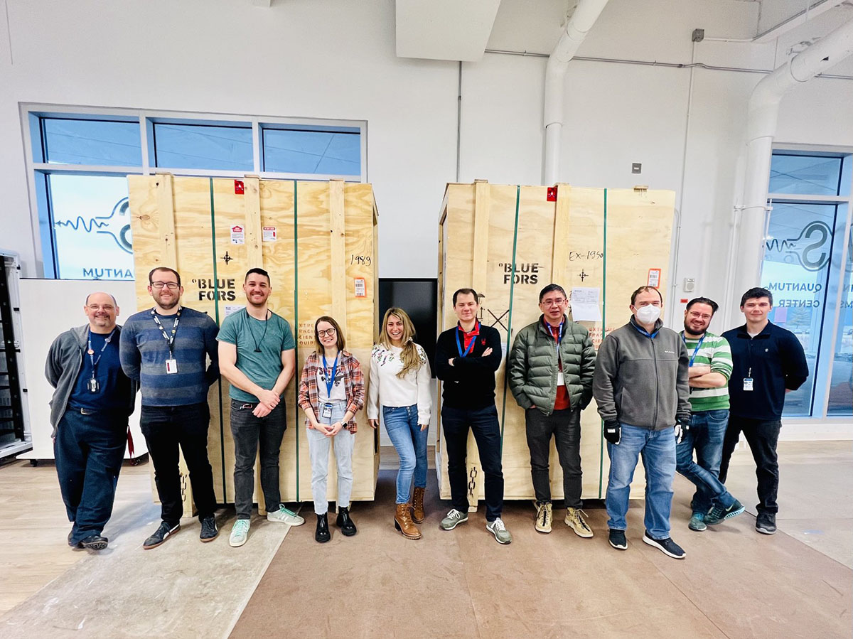
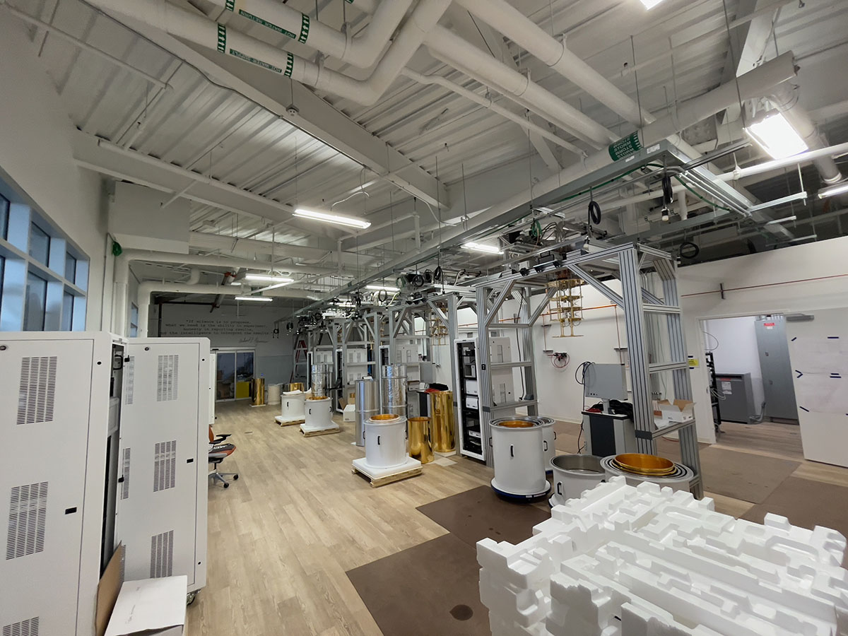
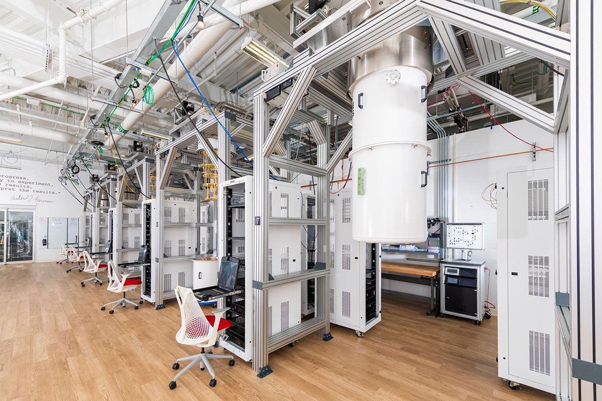
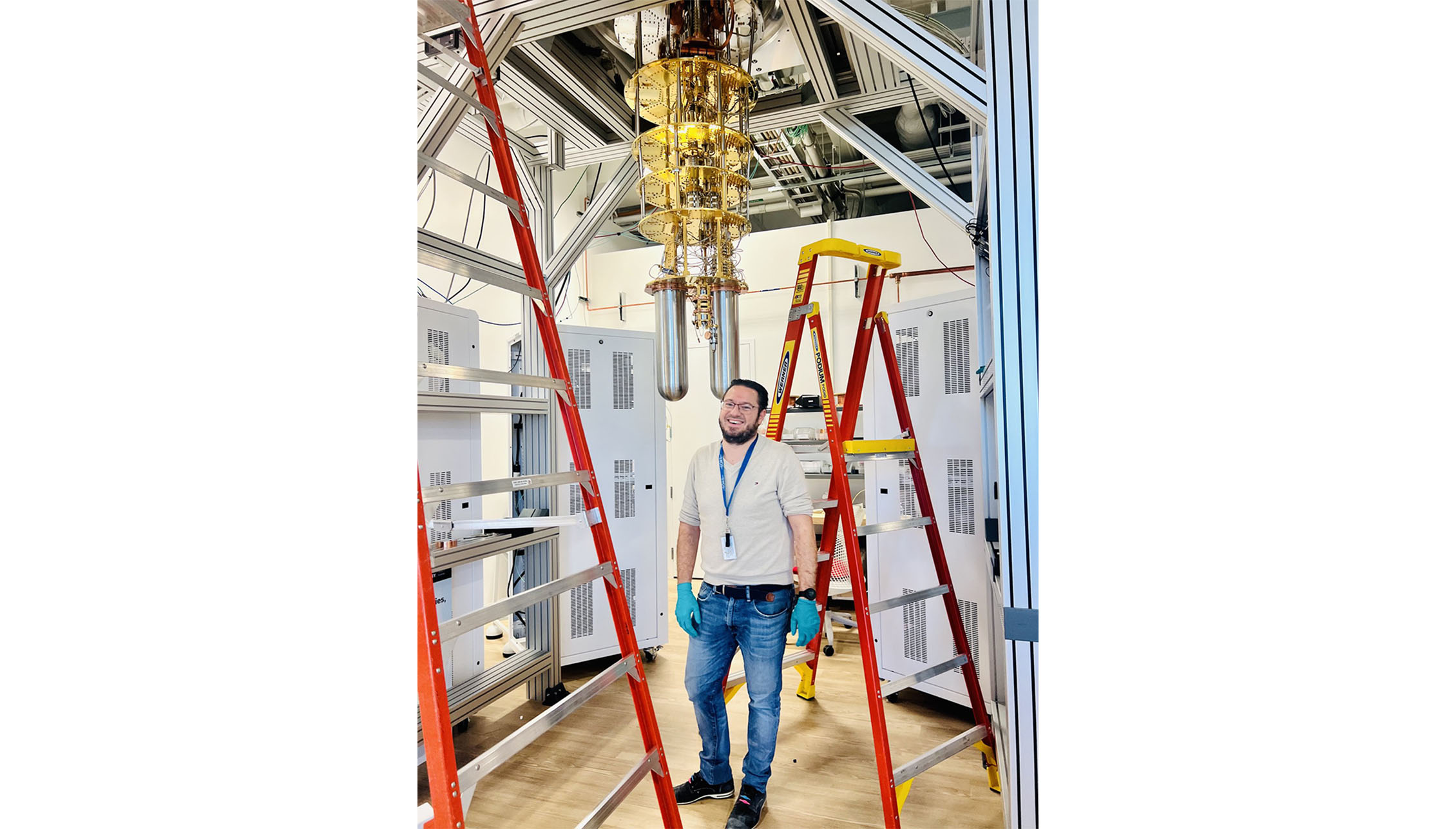
The Quantum Garage is one piece of a broader Fermilab infrastructure supporting quantum systems, superconducting materials and devices, high-magnetic-field experiments and cryogenic technologies needed for future scale.
SQMS also built a distributed laboratory that connects complementary capabilities across partner institutions, from device fabrication and atomic-scale materials characterization to specialized qubit testbeds and unique experimental environments.
Together, these facilities form a scientific tool chain — from materials to devices to systems to experiments — distributed across institutions and connected by a common mission.
Building bridges between people
When I think about SQMS today, I increasingly think of it as a network of human connections. The collaboration was intentional from the beginning. No single institution, and certainly no single scientific discipline, possesses all the expertise required to solve the problems involved in scaling quantum systems.
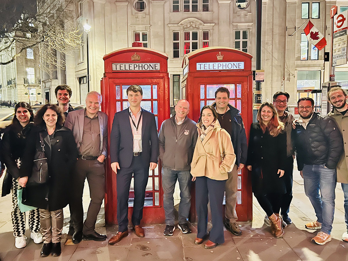
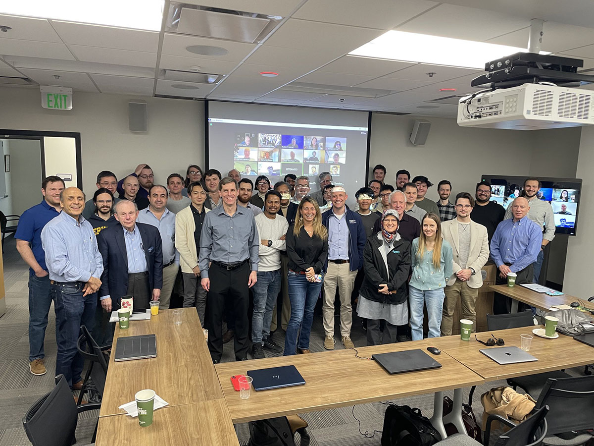
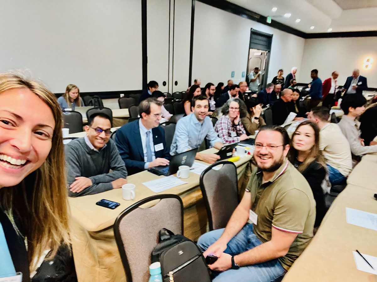
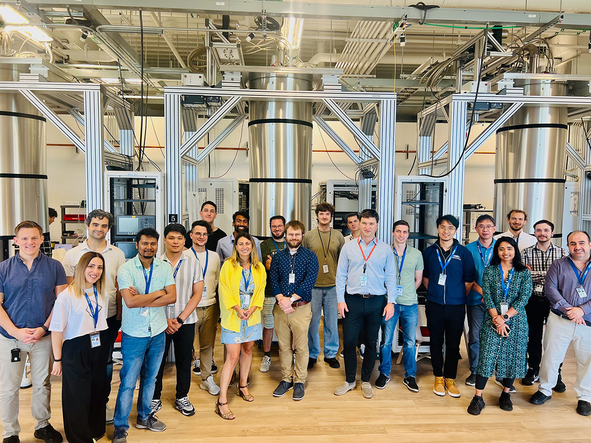
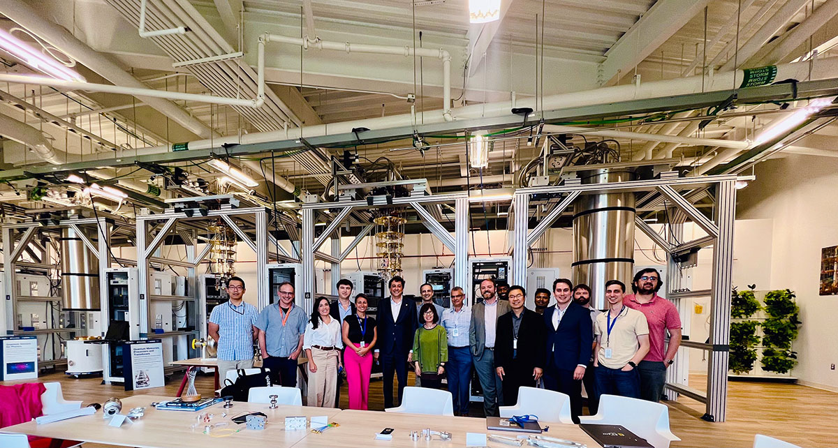
SQMS therefore embraced a simple model: identify the problem first, then bring together the people with the capabilities needed to solve it, regardless of where they work or what field they come from. To me, this is what a national research center should do at its best. It should not simply distribute work among institutions. It should make the boundaries between them scientifically permeable.
Training a workforce by doing the work
The same philosophy has shaped how I think about workforce development. Some of the most powerful training happens by giving people difficult, important problems and the opportunities to solve them alongside experts from other fields.
Our students and postdocs are not watching quantum science from the sidelines. They are building devices, operating qubits in dilution refrigerators, characterizing materials, developing algorithms, collecting data, commissioning experiments and writing the papers that advance the field. In doing that work, they learn how materials, devices, engineering, computing and scientific applications fit together.
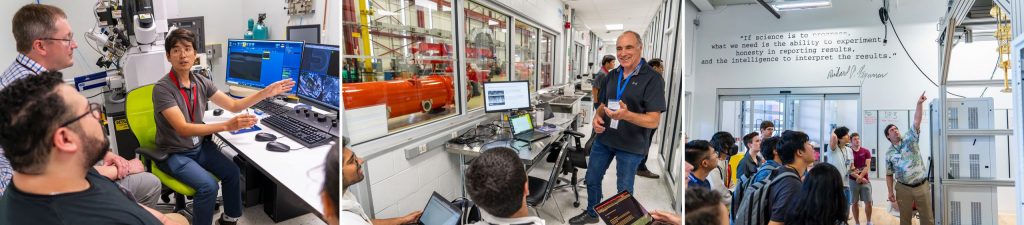
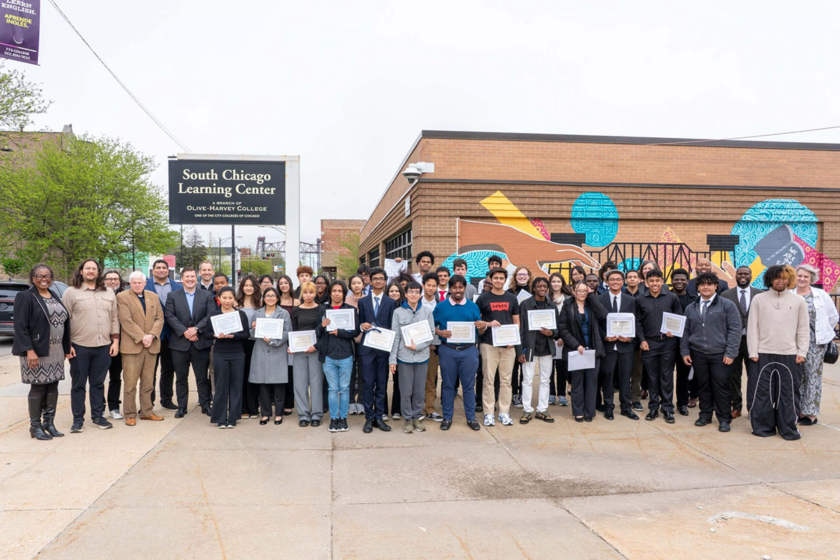
We have also worked to extend that experience beyond the center. In 2023, SQMS hosted the inaugural U.S. Quantum Information Science Summer School, which brought together 150 undergraduate and graduate students and professionals from national laboratories and industry, supported by more than 40 instructors. Participants combined classroom learning with hands-on experience in superconducting qubit and radio-frequency measurements, materials characterization and quantum algorithms.
That is the kind of workforce development I believe we need: not only teaching quantum science but teaching people how to do quantum science together.
Growing an ecosystem
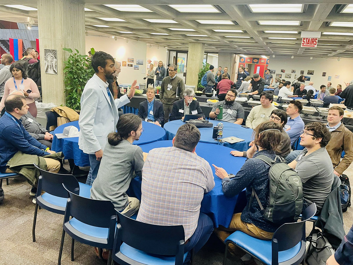
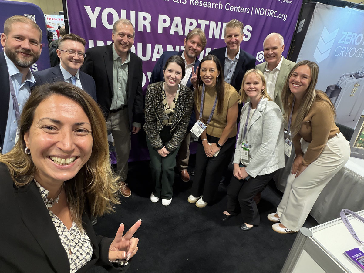
Over time, the community around SQMS has grown well beyond the center’s formal boundaries. When we inaugurated the Quantum Garage in 2023, the first day of the SQMS annual meeting became an “Ecosystem Day,” bringing more than 300 people to Fermilab. By 2025, during the International Year of Quantum Science and Technology, that idea had grown into “Exploring the Quantum Universe,” which brought together researchers, students, industry, national laboratories, government and the public to discuss both the science and what the field would need next.
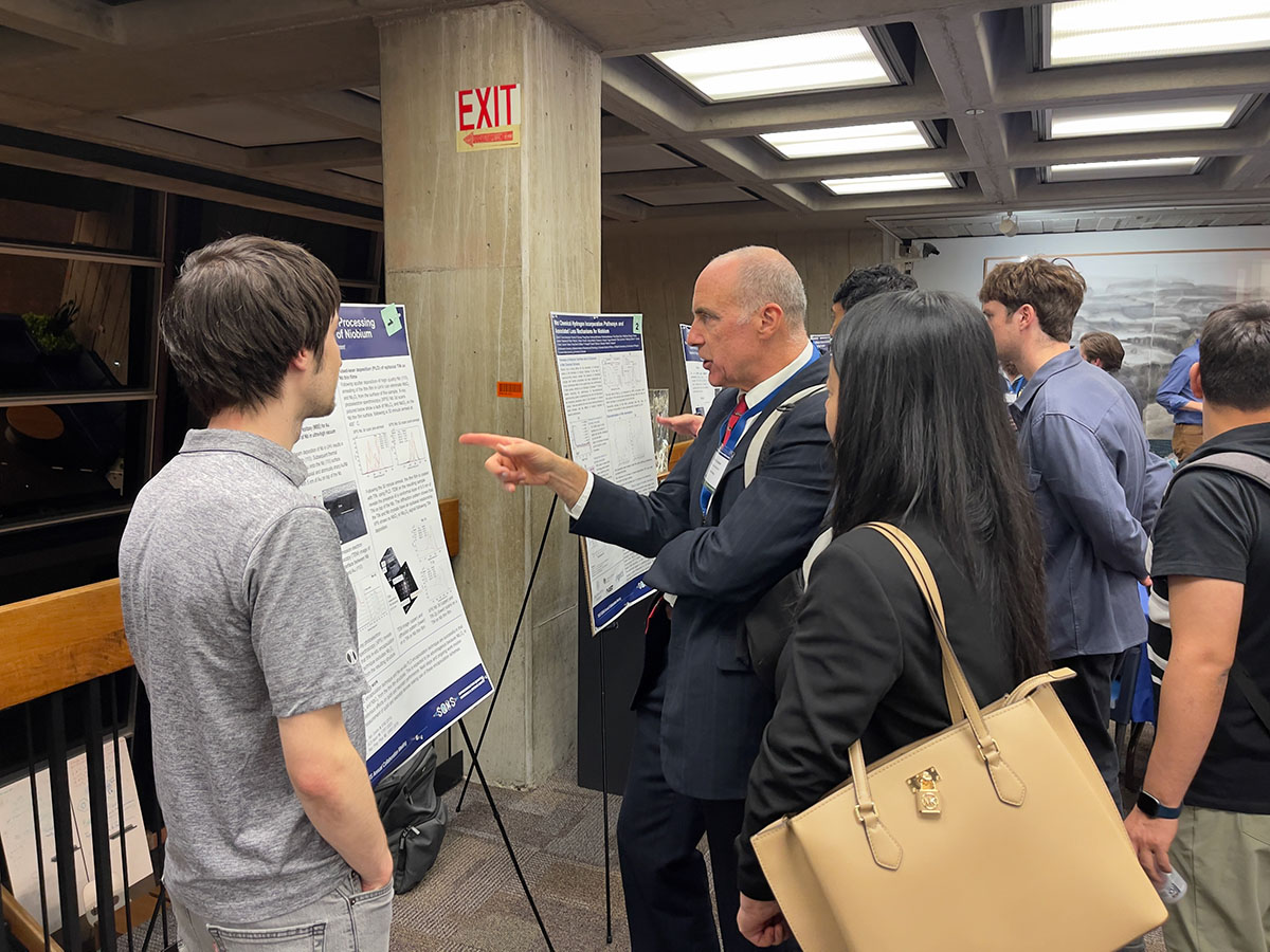
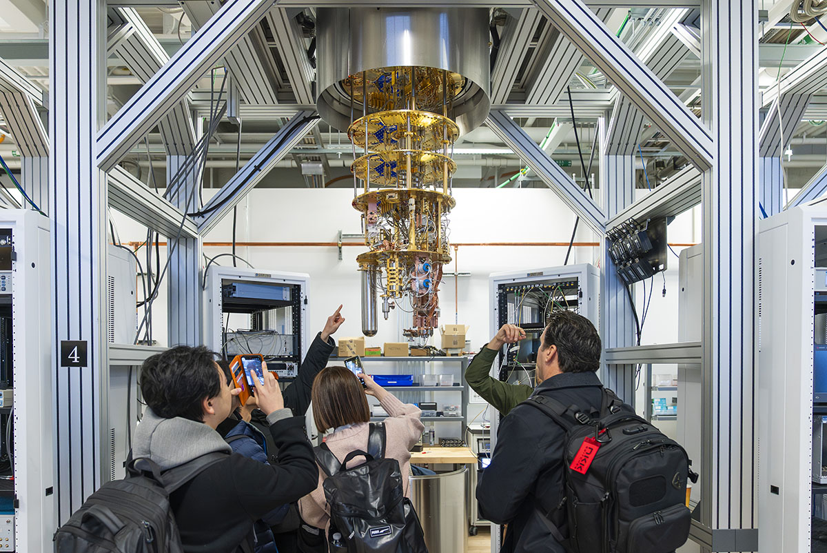
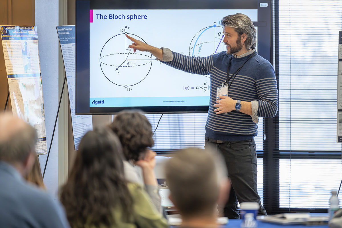
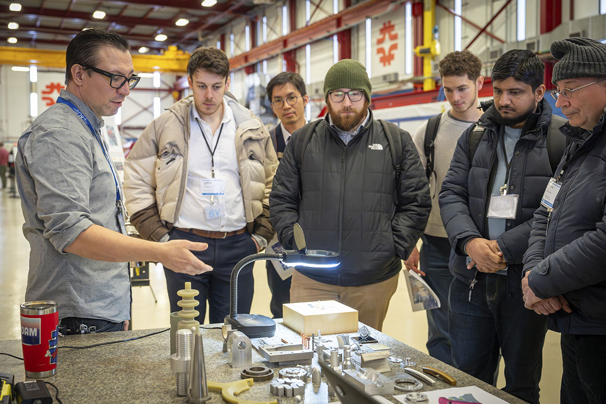
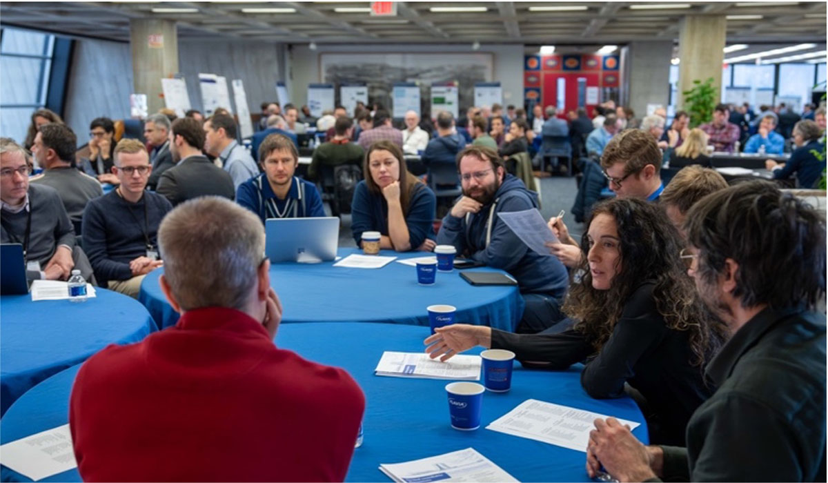
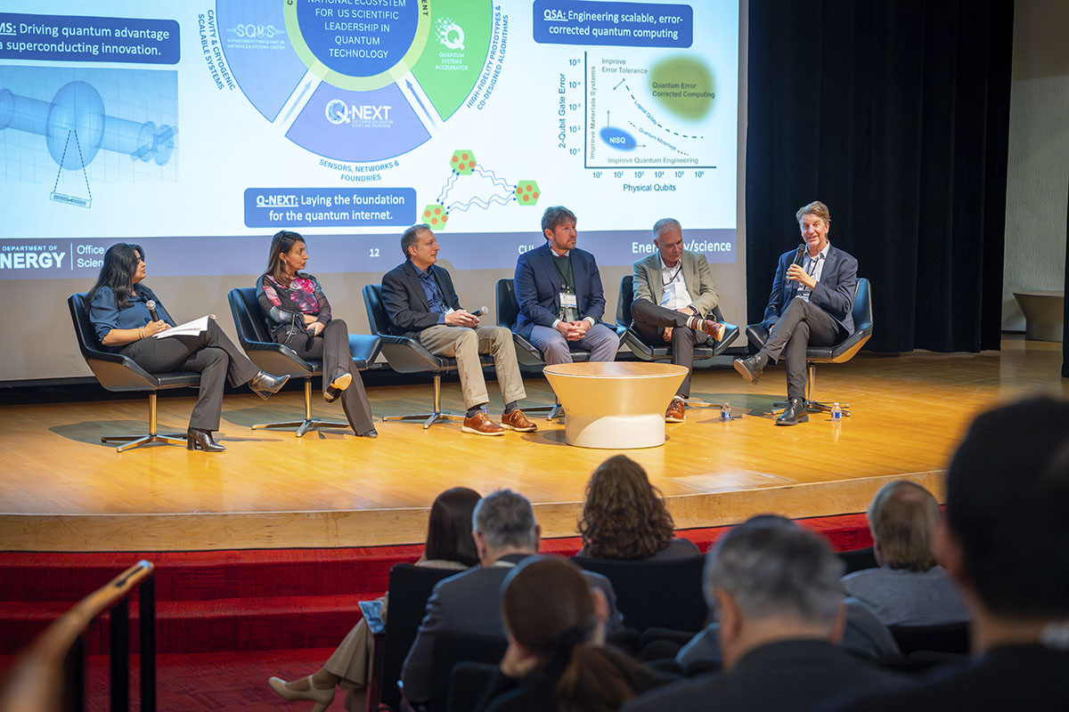
That community will be increasingly important as quantum technology moves toward larger, more integrated systems. The next stage will require not only advances in individual technologies, but facilities sophisticated enough to bring them together and make them accessible to scientists who want to use quantum systems to pursue their own scientific questions.
Looking around SQMS today, at the laboratories we have built, the people we have trained, and the relationships connecting universities, national laboratories and industry, I realize that we have spent six years building many of the ingredients of exactly that future.
We built devices. We built laboratories. We built capabilities that did not exist before. But above all, we built connections — and those connections may ultimately be the most important infrastructure we leave behind.
Fermi National Accelerator Laboratory is America’s laboratory for particle physics and accelerator research. Fermi Forward Discovery Group manages Fermilab for the U.S. Department of Energy Office of Science. Visit Fermilab’s website at www.fnal.gov and follow us on social media.
The Superconducting Quantum Materials and Systems Center at Fermilab is supported by the DOE Office of Science.
The Superconducting Quantum Materials and Systems Center is one of the five U.S. Department of Energy National Quantum Information Science Research Centers. Led by Fermi National Accelerator Laboratory, SQMS is a collaboration of more than 40 partner institutions — national labs, academia and industry — working together to bring transformational advances in the field of quantum information science. The center leverages Fermilab’s expertise in building complex particle accelerators to engineer multiqubit quantum processor platforms based on state-of-the-art qubits and superconducting technologies. Working hand in hand with embedded industry partners, SQMS will build a quantum computer and new quantum sensors at Fermilab, which will open unprecedented computational opportunities. For more information, please visit www.sqmscenter.fnal.gov.
Fermilab editor’s note: The following press release was posted by the U.S. Department of Energy.
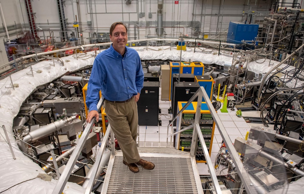
Charles “Chris” Polly has been a central figure in Muon g-2 experiments for almost three decades. His leadership and contributions were key to achieving the most precise measurement of the anomalous magnetic moment of the muon in particle physics to date, with the latest result published in 2025.
He was a lead graduate student on the Muon g-2 experiment at Brookhaven National Laboratory. The Brookhaven result, completed in the early 2000s, revealed a tantalizing discrepancy between experiment and theoretical predictions, making it one of the most closely watched measurements in particle physics and motivating decades of further research.
Polly was instrumental in the move of the 50-foot muon storage ring from Brookhaven National Laboratory in New York to Fermilab in Illinois. He helped lead the next generation of the Muon g-2 experiment at Fermilab as the Project Manager who led the design and construction of the experiment from start to finish, and later served as co-spokesperson when the collaboration announced its first result in 2021.
U.S. Secretary of Energy Chris Wright today announced nine recipients of the prestigious Ernest Orlando Lawrence Award for their exceptional contributions to research and development supporting the U.S. Department of Energy’s (DOE) missions in science, energy, and national security.
“This year’s Lawrence Award recipients exemplify the ingenuity and determination that drive America’s leadership in science and technology,” said U.S. Secretary of Energy Chris Wright. “From achieving fusion ignition to advancing critical materials and high-performance computing, these scientists and engineers are tackling some of our nation’s most complex challenges and translating groundbreaking research into real-world capabilities. Their work strengthens our nation’s energy security, drives American innovation, and ensures the United States remains at the forefront of scientific discovery.”
Established in 1959, the Lawrence Award recognizes mid-career U.S. scientists and engineers for groundbreaking achievements across nine scientific and engineering categories. The award is among the longest-running and most prestigious science and technology honors bestowed by the U.S. government.
The 2026 Ernest O. Lawrence Award recipients are:
Charles “Chris” Polly, Ph.D. (Fermi National Accelerator Laboratory) – High Energy Physics – Honored for his “exceptional scientific and technical contributions to low-energy precision measurements in particle physics, most notably leadership of the experimental measurement of the anomalous magnetic moment of the muon with the Muon g-2 experiment.”
Eric J. Schelter, Ph.D. (University of Pennsylvania) – Atomic, Molecular, and Chemical Sciences – Honored for his “fundamental chemical studies of energy-critical metals leading to new methods for their selective and sustainable separations.”
Patrick Chain, Ph.D. (Los Alamos National Laboratory and New Mexico Consortium) – Biological and Environmental Sciences – Honored for his “pioneering work in genomics and microbiome science, including discoveries of new bacterial-fungal interactions and revolutionizing the field by democratizing access to advanced bioinformatics tools.”
Samuel W. Williams, Ph.D. (Lawrence Berkeley National Laboratory) – Computer, Information, and Knowledge Sciences – Honored for his “pioneering contributions in performance modeling, hardware/software design optimization, and novel computer architecture for high-performance computing, enabling modeling of complex computational solutions, and increasing analysis speed, simulation accuracy, and computational efficiency.”
Thomas Epps, III, Ph.D. (University of Delaware) – Condensed Matter and Materials Sciences – Honored for his “fundamental contributions to chemistry and materials science with applications in the chemical upcycling of polymeric waste, generation of high-performance materials from biomass feedstocks, and development of membranes for lithium-ion battery technologies.”
Gregg Beckham, Ph.D. (National Laboratory of the Rockies and University of Colorado Boulder) – Energy Science and Innovation – Honored for his “transformative research in the conversion of lignocellulosic biomass and waste plastics via biology, chemistry, and engineering, yielding building blocks for sustainable fuels, chemicals, and materials.”
Andrea L. Kritcher, Ph.D. (Lawrence Livermore National Laboratory) – Fusion and Plasma Sciences – Honored for her “exceptional design efforts leading to the first-ever achievement of fusion ignition in the Laboratory, which is of major scientific impact to institutional and national missions, the private sector, and fusion interests within academia.”
Michael Reed, Ph.D. (Nevada National Security Site) – National Security and Nonproliferation – Honored for his “vital contributions to national and international nuclear emergency response through the Advanced Visualization & Integration of Data (AVID) software, which broke existing paradigms by simultaneously fusing all radiological data into a single interface connected seamlessly to world-wide expertise.”
Lijuan Ruan, Ph.D. (Brookhaven National Laboratory) – Nuclear Physics – Honored for her “outstanding leadership and ingenuity in the design, construction, and operation of novel detector systems in the STAR experiment, transforming dilepton final states into precision probes of heavy ion collisions.”
DOE will honor the recipients at a hybrid award ceremony in Washington, D.C., on November 13, 2026. The ceremony will be broadcast live online, and a recording will be available following the event. Registration is required for both virtual and in-person attendees. Due to space and security requirements, in-person attendance is limited, with registration closing October 30, 2026.
For more information and to RSVP, visit the DOE Office of Science Ernest O. Lawrence Award webpage.
Decades of pioneering work to create powerful superconducting magnets for particle physics research also laid the foundation for technologies that have benefited society, such as MRI machines used for medical imaging. Since building the Tevatron, once the world’s most advanced particle collider, Fermi National Accelerator Laboratory has developed expertise across advanced superconducting materials, magnet prototypes, diagnostics tools and analysis tools.
Now, Fermilab is launching the MAGNet Environment Simulator, or MAGNES. Jointly funded by the DOE Office of Fusion and the DOE Offices of High Energy Physics and Nuclear Physics, it will support research aimed at harnessing nearly limitless fusion energy.
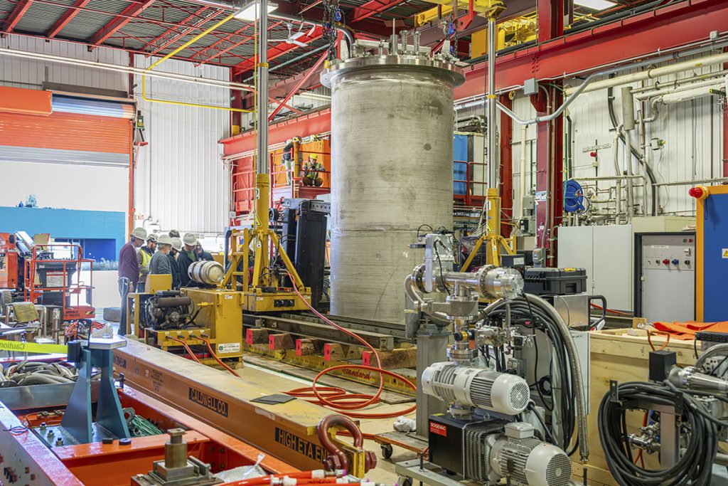
The latest advances in magnet technologies often pull particle physics and fusion research together. Fermilab has spent decades designing and building some of the most powerful superconducting magnets in the world for particle accelerators. Fusion reactors — particularly the tokamak designs at the frontier of research — require similarly powerful magnets to confine the superheated plasma where fusion reactions occur. Fermilab’s combination of magnet engineering expertise, test infrastructure, and scientific depth makes it a natural partner for the global push toward fusion energy.
Testing superconducting cables in an advanced cryogenic facility
According to Greek legend, a shepherd named Magnes first discovered the phenomenon of magnetism when the iron in his staff and sandals became attracted to a naturally magnetic rock, later known as lodestone. That ancient observation inspired the concept — and ultimately the word — magnetism. Over the centuries, this simple curiosity evolved into one of the most transformative forces in science and technology, culminating in the 20th-century discovery of superconductivity, which made possible the powerful magnets that underpin modern particle accelerators, fusion devices and medical imaging.
“We chose the name MAGNES to reflect both the history and the future of magnetism,” said Stephen Gourlay, director of the Magnet Technology Division at Fermilab. “For a facility dedicated to advancing extreme-field superconducting magnet technologies for fusion energy and particle accelerators, it provides both an appropriate foundation and an inspiration for the breakthroughs yet to come.”
Certain materials, when cooled to extreme temperatures, lose all electrical resistance and can carry extraordinary currents, making them capable of generating magnetic fields far beyond what conventional electromagnets can achieve. Today, superconducting magnets are essential to both high energy physics and fusion energy research.
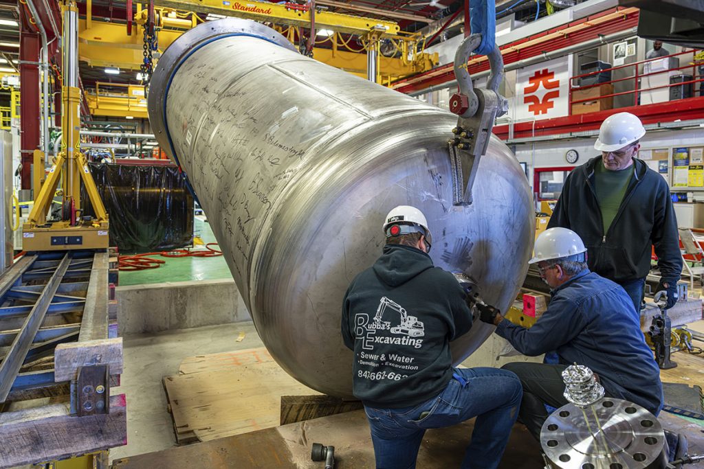
In particle accelerators, magnetic fields are used to steer charged particles toward their targets; in fusion research, magnetic fields confine the intensely hot plasma necessary to facilitate and sustain nuclear fusion reactions. Cables made from superconducting materials could carry the strong electrical currents required for magnets inside a future fusion reactor. If researchers can use powerful magnetic fields to reliably control sustained fusion reactions, they could set the stage for a method to generate nearly limitless energy by replicating the same nuclear process that powers the Sun.
The MAGNES test bed at Fermilab will be unique in the United States for its ability to provide access to a volume of high magnetic field that can be used for testing the superconducting cables that would go into such a reactor.
MAGNES will also help us explore the upper limits of operational temperatures for superconductors, since higher temperatures could widen the application of superconducting materials and lower the costs of running cryogenic systems used to cool the materials.”
Stephen Gourlay, Magnet Technology Division director
“MAGNES is designed to simulate the environment that cables would experience inside a magnet,” said Gourlay. “The test magnet provides a strong, stable background magnetic field, and we pass current — up to 100,000 amps — through the superconducting cables to test their performance in realistic conditions. MAGNES will also help us explore the upper limits of operational temperatures for superconductors, since higher temperatures could widen the application of superconducting materials and lower the costs of running cryogenic systems used to cool the materials.”
The controlled environment of MAGNES is also designed with safety in mind. When a superconducting cable is pushed beyond its limits, it undergoes a rapid transition called a “quench” — a sudden loss of superconductivity that releases energy. Understanding and managing this process safely is critical before any cable design can be used in a fusion reactor. This testing capability enables researchers to push cables to their performance limits, setting the stage for deeper analysis of how much current the materials can sustain before losing their superconducting properties.
“By testing the critical current-carrying capacity of these cables, we can determine how much current they can handle before they lose their superconducting properties, which depend on the background magnetic field,” said Yuhu Zhai, principal engineer at Princeton Plasma Physics Laboratory. “With a higher background field, we can use lower power supplies to test these cables.”
At the heart of MAGNES is a powerful magnet designed and fabricated by Lawrence Berkeley National Laboratory. It features an extra-large bore to accommodate the high-current cables and also facilitate a wide variety of other experiments.
“The 15-tesla dipole magnet made by Berkeley Lab — about 300,000 times stronger than Earth’s magnetic field — will be installed in an 18-foot-deep and nearly 5-foot-diameter pit that can reach temperatures colder than outer space,” said Gueorgui Velev, of Fermilab’s Magnet Technology Division.
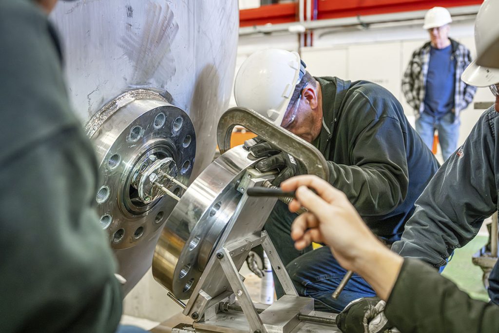
To put that field strength in perspective, a typical hospital MRI machine generates between 1.5 and 3 tesla. At 15 tesla, MAGNES can recreate the intense magnetic environment that superconducting cables would experience deep inside a next-generation fusion reactor — conditions that no other U.S. facility can currently replicate for cable testing at this scale.
MAGNES’ cryostat — the system that chills samples to roughly 2 to 4 degrees above absolute zero — was built by a company in Illinois. Senior Fermilab engineer Vlad Nikolic coordinated the cryostat design and construction.
“This unique system required precise machining in critical areas. The cryostat — which cools the magnet — needs an especially precise seal where superfluid helium meets normal liquid helium. That seal must be flat to within two-thousandths of an inch across a 14-foot circumference,” said Nikolic.
“Now that we’ve carefully installed the cryostat, our next step is to build the anti-cryostat, which enables temperature control of test samples from cryogenic to room temperatures.”
Vlad Nikolic, senior engineer
“Now that we’ve carefully installed the cryostat, our next step is to build the anti-cryostat, which enables temperature control of test samples from cryogenic to room temperatures,” Nikolic continued. “The anti-cryostat allows us to change the sample’s temperature without warming up the main magnet that generates the background magnetic field. Without it, warming the magnet would take about a month. With the anti-cryostat, the sample can be changed in just one day.”
This ability to test samples across a spectrum of temperatures allows researchers to map how cable performance changes under different thermal conditions and magnetic fields — critical data for fusion reactor design. As cables warm, their current-carrying capacity falls and the risk of quenching rises. By quantifying exactly where those thresholds lie, researchers can determine whether a given cable material is suitable for a reactor’s operating environment, and whether new high-temperature superconductors might eventually replace more costly, harder-to-cool alternatives.
With construction of MAGNES well underway and the first cable tests expected to begin in the summer of 2028, Fermilab is positioning itself as a key player in the Department of Energy’s push to achieve sustainable and scalable fusion energy. The facility’s research will directly inform the design of magnets for next-generation fusion devices, providing the foundational data that government labs, universities and private fusion companies need to move from prototype to power plant. In doing so, Fermilab’s decades-long legacy of magnet innovation may prove as consequential to the future of energy as it has been to the frontiers of physics.
Fermi National Accelerator Laboratory is America’s national laboratory for particle physics and accelerator research. Fermi Forward Discovery Group manages Fermilab for the U.S. Department of Energy Office of Science. Visit Fermilab’s website at www.fnal.gov and follow us on social media.