Olivia Seidel is tackling a problem that sounds deceptively simple: understanding how transistors behave when they get very cold. The answers she finds could shape everything from quantum computers to satellites in outer space, and she is using artificial intelligence to accelerate that research.
A Ph.D. student working within Fermi National Acceleratory Laboratory’s Microelectronics group, Seidel is leveraging AI for cryogenic transistor modeling. Her work draws on Fermilab’s deep expertise in microelectronics and cryogenic devices to support key goals of the Genesis Mission — a sweeping national AI initiative combining the expertise of the Department of Energy’s national laboratories, U.S. research universities and industry to supercharge American innovation.
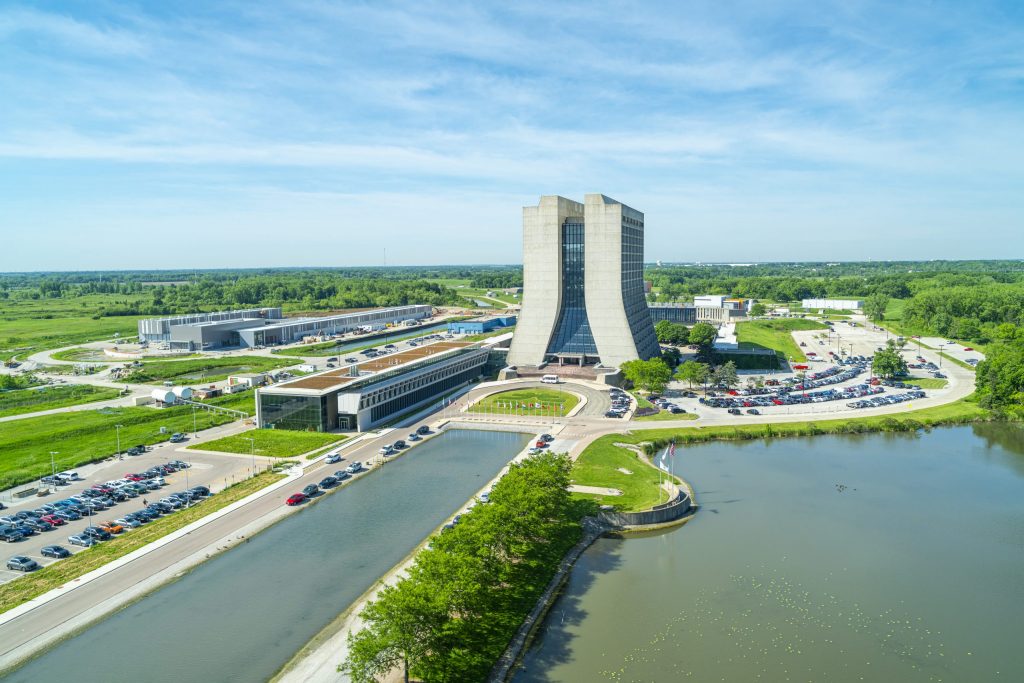
I recently visited Seidel at her office in Fermilab’s iconic Wilson Hall to talk about the exciting work underway.

Q: What exactly is a transistor, and why should anyone care about how it behaves in the cold?
Transistors are the computational building blocks of every electronic device you use — your phone, your laptop, anything that manipulates bits and bytes. Over decades, industry has become extraordinarily good at making them smaller and more powerful. We’re talking about transistors just a few nanometers across — so small that a single wavelength of visible light is hundreds of times wider.
For most of that history, room temperature was the only environment that mattered. But quantum computing and other emerging technologies require electronics that function at cryogenic temperatures — just a few degrees above absolute zero. And at those extremes, transistors behave very differently.
Q: How do the transistors behave differently?
One of the clearest examples is what it takes to switch a transistor on. At room temperature, you apply a certain voltage, and it turns on. At deep cryogenic temperatures below 4 kelvin [about minus 452 degrees Fahrenheit], like the temperatures of outer space, it takes significantly higher voltage to flip that switch. The whole curve of the transistor’s behavior shifts.
That might sound like a minor technical detail, but if you’re a circuit designer unaware of that shift, your entire circuit can fail. It could also technically work while consuming far more power than it should — and in a cryogenic environment, excess power means excess heat, which can be catastrophic. Heat causes decoherence in quantum systems, essentially causing quantum properties to fall apart, and can disrupt electronics trying to detect neutrinos in a cryogenic liquid-argon environment.
Q: Do you build the models that predict this behavior?
I do! I build physics models that accurately describe how transistors behave at cryogenic temperatures, and we measure transistors in the lab at those temperatures to inform and validate the models. The goal is that when a circuit designer sits down to build something that needs to operate at 4 kelvin, they can trust the model — rather than building the whole thing, putting it in a cryogenic system and finding out it doesn’t work.
Q: What are some of the real-world applications that would benefit from this knowledge?
There are several. One big area is trapped ion quantum computing. Ions — charged atoms — can serve as qubits, and to manipulate them precisely, you use high-voltage transistors in an extremely cold environment. The cold suppresses thermal noise, helping preserve the fragile quantum state of the qubit.
Another application is superconducting nanowire single-photon detectors, or SNSPDs — thin superconducting films that detect single particles of light. These are used for particle detection and precision measurements and also require electronics that function at deep cryogenic temperatures.
There’s also interest in using cryogenic transistors for the readout and control of superconducting qubits — having electronics that live inside the cryogenic system itself rather than sending signals back up to room temperature. Along with quantum applications, there are particle physics uses at Fermilab, like the large liquid-argon detectors in the DUNE at LBNF neutrino experiment, and interest from deep space satellite designers where the background temperature of the universe sits around 3 kelvin [about minus 454 degrees Fahrenheit].
Q: That’s a wide range of applications. How long does it currently take to build these models?
That’s the problem. Using standard industry tools, building a robust set of cryogenic physics models for one type of transistor can take around two years. Technology advances faster than the models do — and that’s an industry-wide challenge.
Q: Is this where AI and machine learning can come in?
Through the Genesis Mission, DOE is harnessing capabilities at the national laboratories by using AI to make laborious, data-rich research processes dramatically faster. Our work on cryogenic transistor modeling is a direct example.
The idea is to use machine learning to speed up the modeling process enormously. Instead of painstakingly fitting physical parameters using other tools, we let the AI/ML model directly predict the model from the measurement data we collect in the lab.
As a proof of concept, I built a prototype that replaces one step in the traditional modeling process with a machine learning approach, yielding results just as good, if not better, than the conventional method.
The key metric is the time required to go from an undefined set of physics-model parameters to a complete, working parameter set tailored to a given transistor and capable of accurately predicting its deep-cryogenic behavior.
“We’re laying the groundwork so that future researchers don’t have to spend years on something a well-trained model can do in a fraction of the time.”
Olivia Seidel
Using the new machine learning approach, I spent roughly two weeks generating training data and building the model. Once trained, it predicts optimal physics parameters from deep cryogenic transistor measurement data in approximately 120 milliseconds. The conventional approach, by contrast, can take anywhere from weeks to months, depending on the transistor.
That prototype is a core aspect of the Accelerating eXtreme Environment Specs-to-Silicon project led by Fermilab — a Genesis Mission initiative advancing microelectronics in extreme environments where industry expertise and investment remain scarce. We’re using my work to build a complete deep cryogenic model for transistors highly sought after for quantum information science and high energy physics applications at 4 kelvin. The goal is a full, production-quality model built from the ground up using AI — not just adapting a room-temperature model and hoping it holds at cryogenic temperatures.
Q: What does “from the ground up” mean in this context?
Currently, the standard approach is to take a room-temperature transistor model and adapt it to cryogenic temperatures, re-extracting all the physics parameters to fit what you actually measure. It works, but it’s slow and laborious.
The longer-term vision is to build models starting from the material properties of the transistor itself — not from a room-temperature approximation. The machine learning model would infer the underlying physics directly from lab measurements, rather than adjusting a pre-existing framework. It’s a fundamentally different and more powerful approach.
Q: What do you think about the significance of this work within the broader picture?
Cryogenic transistor modeling was something that wasn’t at the forefront of our thinking about twenty years ago. Now it’s increasingly critical infrastructure for quantum computing, particle physics and space technology — and the demand is only going to grow.
What we’re doing with machine learning is similar to how Fermilab once automated wire bonding — a precise, painstaking manual process of connecting tiny wires to chips by hand. Eventually machines took over, freeing skilled people to focus on harder problems. We’re laying the groundwork so that future researchers don’t have to spend years on something a well-trained model can do in a fraction of the time. It’s not replacing the science — it’s making the science move faster.
Fermi National Accelerator Laboratory is America’s national laboratory for particle physics and accelerator research. Fermi Forward Discovery Group manages Fermilab for the U.S. Department of Energy Office of Science. Visit Fermilab’s website at www.fnal.gov and follow us on social media.
Physicists discovered decades ago that odd little particles called neutrinos, of which there are three known “flavors,” morph between these flavors as they travel, and they call this phenomenon neutrino oscillation. The Deep Underground Neutrino Experiment, developed by an international collaboration and hosted by Fermi National Accelerator Laboratory, aims to answer fundamental questions about the early evolution of the universe through its study of these oscillations. This requires a neutrino beam and the ability to sample the neutrinos right out of the gate in their original state and again after they change.
To capture the data, DUNE is building both a near detector and a far detector in the path of the most intense neutrino beam ever created. The hybrid near detector, located only about 2,000 feet downstream from the neutrino source at Fermilab in Batavia, Illinois, will get the first taste. But most of the neutrinos will travel 800 miles on to the far detector at the Sanford Underground Research Facility in Lead, South Dakota, where only a small proportion will interact with the detector because the beam will spread out over that distance and neutrinos are famously elusive. The rest will harmlessly sail on, largely unimpeded, through the Earth’s crust and beyond.
Since the DUNE far detector will use liquid-argon time projection chamber technology to measure neutrinos, it is critical that the same technology be used for the near detector to facilitate a comparison of data on the same target — liquid argon. This part of DUNE’s near detector is called ND-LAr, short for “near detector liquid argon.”
“Despite being only 1% the size of one far detector module, this ND-LAr detector is still large enough to fully contain the signals from neutrinos.”
Michele Weber, the University of Bern
As part of DUNE’s plan to measure neutrinos over a wide range of energies, the ND-LAr, along with an accompanying muon spectrometer, will be able to move sideways off axis to better characterize the beam. A stationary beam monitor will remain on axis to watch for any beam variations that could affect measurements.
“Despite being only 1% the size of one far detector module, this ND-LAr detector is still large enough to fully contain the signals from neutrinos,” said Michele Weber from the University of Bern who is also the leader of the ND-LAr consortium. “This enables a precise comparison with what is seen at the far detector, thereby revealing the neutrino oscillation that occurs between the two sites.”

Given that the neutrino beam broadens with distance, more like the light from a flashlight than a laser beam, the near detector will see a much more concentrated flux of neutrinos than will the far detector — one of the reasons the near detector does not have to be so large. This concentration of neutrinos leads to a phenomenon called “pileup” in the detector, where the rate of neutrino interactions overwhelms the rate at which the detector can record the charge signals that emanate from them. The ND-LAr design cleverly mitigates this problem by segmenting its volume into mini detectors, called modules, with individual pixelated readout. The numerous interactions occur in different modules, without overwhelming any of them.

ND‑LAr uses the novel liquid-argon pixel system, or LArPix, that was invented by physicists and engineers at Lawrence Berkeley National Laboratory. This end‑to‑end pixelated sensor and electronics system can image neutrino events in true 3D, which is an important aspect to resolving individual neutrino interactions in the detector.
Brooke Russell, a researcher with the Massachusetts Institute of Technology, is testing reconstruction efforts for this type of pileup mitigation. By anticipating pileup from the neutrino beam, the team hopes to paint as accurate a picture as possible and not be overwhelmed by the rate of neutrino interactions.
“ND-LAr is unique in that we purposely partition neutrino signals across multiple optically segmented volumes and algorithmically stitch these signals back together,” Russell said.
Through these segmentation and reconstruction efforts, DUNE will provide consistent clarity of the recorded neutrino interactions.
Even with the segmentation, interactions that occur very close to one another in space may be misinterpreted as a single event unless light signals are also collected to separate them in time, according to Zoya Vallari of the Ohio State University, an analysis coordinator for the ND-LAr. The instantaneous signals that scintillation light produces in the liquid argon make it possible to distinguish the potentially overlapping charge signals.
“The prototyping program for the DUNE liquid-argon near detector has been wildly successful, advancing multiple novel detector technologies and algorithms for data analysis.”
Dan Dwyer, Lawrence Berkeley National Laboratory
The DUNE ND-LAr team has been developing and prototyping the segmented liquid-argon time projection chamber design, primarily at the University of Bern, in Switzerland, starting in 2016 with a program called ArgonCube to test the component technologies. In 2022 the steadily growing team constructed and tested a demonstrator of four half-size time-projection chamber modules, called 2×2. After collecting data from a neutrino beam source, this detector is now in a non-beam data collection phase at Fermilab, recording events from cosmic rays and other sources, such as calibration data. The effort currently involves more than 100 scientists from roughly 40 institutions.
“The 2×2 program has been pivotal in shaping our software, simulation and analysis frameworks,” said Vallari. “The data we collected is driving progress in calibration, event reconstruction and charge-light matching.”
“The experience gained with 2×2 has enabled us to thoroughly validate the detector concept in a realistic environment,” added Livio Calivers, a freshly minted Ph.D. from Bern. “As a young researcher, it gave me the opportunity to build an experiment from scratch and ultimately analyze real data from neutrino interactions.”
The team built and tested a single full-scale module in 2024 that incorporated improvements guided by insights from the 2×2 effort. A full row of five modules is currently in the works to test production, assembly and integration procedures, aiming for production to start at Fermilab in 2026.

“The prototyping program for the DUNE liquid-argon near detector has been wildly successful, advancing multiple novel detector technologies and algorithms for data analysis,” said Dan Dwyer of Berkeley Lab who is also the technical lead for ND-LAr. “These results give us confidence that we can cope with the very high intensity of the DUNE neutrino beam and achieve DUNE’s ambitious scientific goals.”
Fermi National Accelerator Laboratory is America’s national laboratory for particle physics and accelerator research. Fermi Forward Discovery Group manages Fermilab for the U.S. Department of Energy Office of Science. Visit Fermilab’s website at www.fnal.gov and follow us on social media.
A collaborative research team comprised of U.S. Department of Energy national laboratories and led by Fermi National Accelerator Laboratory aims to revolutionize custom microelectronics design by using artificial intelligence to accelerate development of chips that can function in extreme environments.
The Accelerating eXtreme Environment Specs-to-Silicon — or AXESS — project will boost innovation and national competitiveness, enabling breakthroughs in quantum computing, fusion energy and particle physics.

AXESS is a collaborative endeavor leveraging the strengths of the vast DOE lab complex — including Oak Ridge National Laboratory, Lawrence Berkeley National Laboratory, SLAC National Accelerator Laboratory and Sandia National Laboratories — as well as university collaborators and leading industry partners such as Siemens.
The team is developing proofs of concept for DOE’s Genesis Mission — a national mission to accelerate science through AI.
Fermilab, America’s particle physics and accelerator laboratory, is well-suited to lead this type of work and extend the adoption of rapid chip design to other research areas.
All of this coming together within the Genesis Mission is a great opportunity for Fermilab to team up with others and use AI to significantly accelerate chip design.”
Nhan Tran, head of Fermilab’s AI Program
“Particle detectors must function in some of the most extreme environments in terms of radiation, cryogenic temperatures and speed,” said Nhan Tran, head of Fermilab’s AI Program. “As a result, we’ve built our own custom detectors for many years, and Fermilab has established deep expertise in microelectronics for extreme environments. More recently, we’ve developed tools and methods used across the community to integrate AI onto chips. All of this coming together within the Genesis Mission is a great opportunity for Fermilab to team up with others and use AI to significantly accelerate chip design.”
Custom-designing specialized chips that are critical to scientific research is a highly iterative, time-intensive process that can take many months — even years — to complete.
Through this proposed Genesis Mission project, the research team is building a framework that uses AI to speed up the chip-design process, dramatically reducing the time from chip specification to fabrication from months to weeks.
“The goal of this framework is to create systems in AI that help designers make the right decisions at each step of the design process, providing feedback for the next set of designers along the pipeline,” said Giuseppe Di Guglielmo, a principal engineer at Fermilab who is co-leading the project.
Traditionally, chips are designed independently in stages, each by a different set of experts. From materials used, transistor and circuit designs, chip architecture, and finally, algorithms that run on the chips, a decision made in one stage might create issues in subsequent stages. Furthermore, the tools used are typically slow and manually operated.

In contrast, researchers on this project are using AI to integrate all stages, ensuring any decision made in one stage optimizes the entire design and opens up traditional bottlenecks. They use one type of AI — large language models — to coordinate and automate manual steps and make high-level decisions, while another type — smaller surrogate models — act as stand-ins for the more complex and time-consuming models.
These surrogate AI models rapidly make predictions, such as how fast the chip will operate, the amount of power it will consume, the performance of the transistors, and so on, through the various stages. Within minutes, they evaluate millions of design options, predict the performance of each and isolate the most promising candidates before sending them through the full design process.
The initial proof of concept is focused on chips used to control quantum sensors, devices and systems. The team has achieved an approximately 500-times speedup for the design phase of the qubit readout algorithm and its implementation as firmware for field-programmable gate arrays. In addition, they have also developed more accurate transistor modeling at 4 kelvin — about minus 450 degrees Fahrenheit — important for operation in quantum environments. Another important area they are studying is radiation-hardened chips for use in high-energy particle physics experiments.
Under the auspices of the Genesis Mission, the researchers hope to expand this effort into a multi-year project.
By uniting Siemens’ proven technologies with the breakthrough science at Fermilab and across the DOE labs, we’re accelerating a new class of chips for quantum, fusion and high-radiation environments — at a speed and scale the nation has never had.”
David Burnette, engineering director at Siemens
“Siemens is putting industrial-grade hardware design solutions behind the Genesis Mission,” said David Burnette, engineering director for Catapult High-Level Synthesis, Siemens Digital Industries Software. “By uniting Siemens’ proven technologies with the breakthrough science at Fermilab and across the DOE labs, we’re accelerating a new class of chips for quantum, fusion and high-radiation environments — at a speed and scale the nation has never had.”
“We are really excited to be able to partner with other DOE labs and industries that have strong and complementary capabilities, bringing all these experts together across microelectronics and AI to make a big push forward for national success,” said Tran.
Fermi National Accelerator Laboratory is America’s national laboratory for particle physics and accelerator research. Fermi Forward Discovery Group manages Fermilab for the U.S. Department of Energy Office of Science. Visit Fermilab’s website at www.fnal.gov and follow us on social media
Fermi National Accelerator Laboratory and the Sanford Underground Research Facility held an event today in Lead, S.D., celebrating a significant milestone for the most ambitious neutrino research experiment in the United States, the Deep Underground Neutrino Experiment at the Long-Baseline Neutrino Facility. The event commemorated the start of 10 million pounds of steel beams being moved a mile underground to build the structural elements that will form DUNE’s detector elements.
“Today represents the start of a pivotal phase for DUNE, the development of the far detector structures in South Dakota,” Fermilab Director Norbert Holtkamp said. “As we advance this historic effort, our focus remains on safety, quality and schedule — in that order — to ensure we successfully deliver on behalf of the U.S. Department of Energy, our nation and the world.”
Holtkamp added, “We at Fermilab are grateful for the support from DOE and the close collaboration of our science partners at SURF, CERN and the many international institutions that are contributing to DUNE.”

CERN, the European Organization for Nuclear Research, provided personnel, expertise and an in-kind contribution of 10 million pounds of steel for the detectors being assembled underground in South Dakota. This is the first time CERN has invested in infrastructure for an experiment outside of Europe.
The steel cryostat materials contributed by CERN for DUNE are scheduled to be moved underground and prepared for installation this summer. This marks an important transition from construction to detector installation and demonstrates the tangible impact of international in-kind contributions to DUNE.
“This important milestone for DUNE is a testament to the strong scientific partnership between CERN and the United States,” said CERN Director General Mark Thomson. “CERN is playing a pivotal role in the development of its prototype detectors and providing the two enormous cryostats for the experiment itself, while the U.S. Department of Energy national laboratories likewise are playing a critical role for CERN with state-of-the-art superconducting accelerator magnets for the High-Luminosity Large Hadron Collider.”

As America’s particle physics laboratory, Fermilab is host to DUNE — a world-leading, flagship experiment that is the largest scientific project supported by the DOE Office of Science and the largest in the United States. The project will study the neutrino, one of the universe’s most abundant yet least understood subatomic particles. DUNE will send the world’s most intense neutrino beam a distance of 800 miles from Fermilab in Illinois to detectors deep underground at SURF, enabling it to explore fundamental questions about the nature of matter, the evolution of the universe and the origin of matter-antimatter asymmetry.
In addition to expanding our fundamental knowledge, neutrino research has the vast potential to drive advances across a range of fields, including national security, communications and medical imaging.
“DUNE is a powerful example of DOE’s commitment to advancing American leadership in science,” said DOE Under Secretary for Science Darío Gil, one of the attendees at today’s event. “On behalf of the entire DOE leadership team, I offer my congratulations to Fermilab and all those involved in this historic initiative, including our partners around the world who helped make this milestone possible.”
Today’s event provided attendees the opportunity to sign one of the steel beams that will be installed underground for DUNE’s first detector module, including a cryostat that will be used to cool thousands of tons of liquid argon to about minus 300 degrees Fahrenheit to capture neutrino interactions with unprecedented precision. Each of the two planned modules will be roughly the size of a five-story building, measuring 216 feet long, 62 feet wide and 60 feet high. Once complete, the two cryostats will each house 17,000 tons of liquid argon nearly a mile underground at SURF.

Mike Headley, the executive director of the South Dakota Science and Technology Authority and laboratory director at SURF, attributes the success of this project to the international collaboration behind this world-class research.
“SURF is proud to be included among the 1,500 scientific collaborators from around the world who are working alongside hundreds of additional engineers and technicians to complete this project,” Headley said. “We’re excited to see the delivery of this steel a mile underground and to assist in the construction of this colossal experiment.”
With the start of the installation of the underground detectors, Fermilab’s priority is to deliver the first neutrino beam to DUNE by 2031.
Fermi National Accelerator Laboratory is America’s national laboratory for particle physics and accelerator research. Fermi Forward Discovery Group manages Fermilab for the U.S. Department of Energy Office of Science. Visit Fermilab’s website at www.fnal.gov and follow us on social media.
The DOE Office of Science is the single largest supporter of basic research in the physical sciences in the United States and is working to address some of the most pressing challenges of our time. For more information, please visit science.energy.gov.
About SURF:
Sanford Underground Research Facility is operated by the South Dakota Science and Technology Authority (SDSTA) with funding from the Department of Energy’s Office of Science. We are America’s Underground Lab. Our mission is to advance world-class science and inspire learning across generations. For more information, please visit www.sanfordlab.org.
About CERN:
CERN, the European Organization for Nuclear Research, is one of the world’s leading laboratories for particle physics. The Organization is located on the French-Swiss border, with its headquarters in Geneva. Its Member States are: Austria, Belgium, Bulgaria, Czech Republic, Denmark, Estonia, Finland, France, Germany, Greece, Hungary, Israel, Italy, Netherlands, Norway, Poland, Portugal, Romania, Serbia, Slovakia, Slovenia, Spain, Sweden, Switzerland and the United Kingdom. Cyprus is an Associate Member State in the pre-stage to Membership. Brazil, Chile, Croatia, India, Ireland, Latvia, Lithuania, Pakistan, Türkiye, and Ukraine are Associate Member States. Japan and the United States of America currently have Observer status, as do the European Union and UNESCO. The Observer status of JINR is suspended in accordance with the CERN Council Resolution of 25 March 2022. For more information, please visit home.cern.