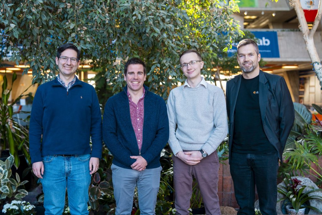
Researchers at the Department of Energy’s Fermi National Accelerator Laboratory, along with scientists and engineers at the computer chip manufacturer Diraq, University of Wisconsin-Madison, University of Chicago and Manchester University, have proposed the development of a quantum sensor made of quantum bits called spin qubits in silicon to probe beyond Standard Model physics. Diraq is a global leader in quantum computing technology on silicon, which is essential to the Quandarum project.
By placing many spin qubits together on a chip to form a sensor, the researchers seek to enable scientists to tease out even the faintest signals from the cosmos. Such a sensor could potentially be used to detect axions, hypothetical particles that some scientists believe comprise dark matter.
Led by Fermilab, the Quandarum project is one of 25 projects funded for a total of $71 million by the DOE program Quantum Information Science Enabled Discovery. The QuantISED program supports innovative research at national laboratories and universities that applies quantum technologies to use for fundamental science discovery.
With this award, researchers plan to develop a novel sensor, bringing together for the first time two specialized technologies: spin qubits in silicon and cryogenic “skipper” analog-to-digital converter circuits used for the readout of dark matter detectors.
Silicon spin-based quantum sensors can provide a powerful platform for testing theories around dark matter because they can exploit quantum interactions to increase sensitivity and explore the limits of what scientists understand about high-energy physics.
It’s all about the spin
Spin qubits store information in the direction of an electron’s spin, a property defined by quantum mechanics. The spin state of an electron is very sensitive to weak electromagnetic fields in the environment, allowing for extremely precise measurements.
“We can’t directly measure what the direction of the spin is, but we can measure small movements of charge because moving charge creates a change in the electric field which can be measured,” said Adam Quinn, Fermilab engineer and project principal investigator.
However, because electron spins are so small, densely packed, and sensitive to even the slightest disturbance, extracting information from spin qubits is quite difficult.
“The core challenge of this sensor is the readout, and the key to success is having the ability to read out information with minimal noise,” said Quinn.
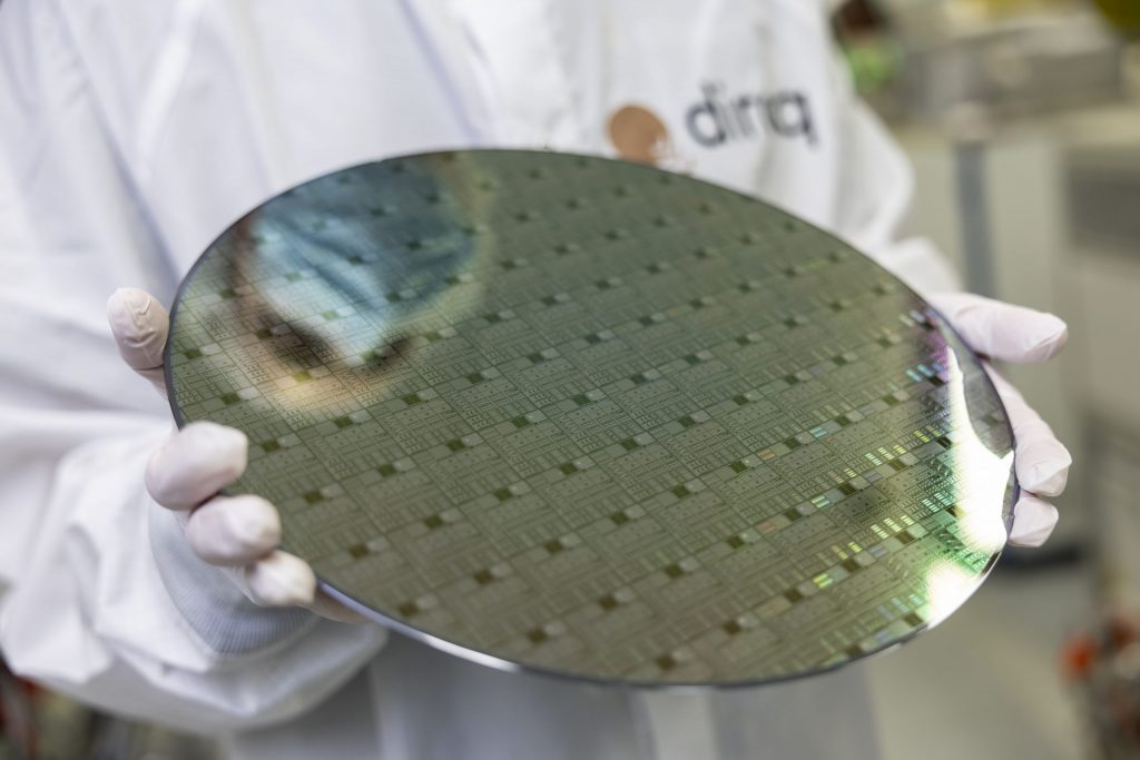
To achieve this, Quinn and his fellow researchers are seeking new ways to use highly scaled readout techniques based on cryogenic application-specific integrated circuits, or ASICs, which would be co-designed using Diraq’s qubit sensor. ASICs are manufactured the same way as the chips that power most electronics today. However, they will use specialized design and layout techniques to achieve superior performance, particularly in extreme environments, such as in a cryogenic chamber.
The Fermilab team is building on prior work at Fermilab on the readout of skipper charge-coupled devices, or skipper CCDs. Engineers developed skipper CCDs to increase the readout accuracy by overcoming noise. By using an action called skipping to move the charge back and forth multiple times, skipper devices enable a more precise measurement at the single-electron level. The Fermilab team plans to apply this innovation to the readout of qubits, with several iterative chip designs that will allow them to more tightly integrate the qubits and readout electronics. They believe this will ultimately lead to a low-power, highly sensitive detector.
Fermilab has been developing novel readout chips for particle physics experiments for many years. Now, engineers and scientists will employ some of these same types of microelectronic circuits and apply them to the development of the new sensor.
Scaling up
However, producing the quantity of qubits needed — potentially thousands — putting them together on a silicon chip, and making them work properly is not easy. During the manufacturing process, each one must be nearly identical and must perform similarly to the others.
Diraq, a company with world-leading expertise indeveloping spin qubits in silicon, is one company that is well positioned to manufacture spin qubits at the scale needed. Silicon is the preferred material because the industrial infrastructure to produce it is firmly established.
“In addition to quantum computing, the inherent characteristics and material properties of silicon spin-based qubits offer significant promise for large quantum-sensing array technology and particle detection applications,” said Andrew Dzurak, founder and CEO of Diraq.
“By utilizing high-precision fabrication processes we are looking to enable the production of quality controlled integrated silicon spin qubits at cost-effective and commercial volumes. This technology has the potential to underpin the development not only of large-scale quantum computers but large-scale quantum sensing platforms,” he said.
One step at a time
Over the next five years, the goal is to combine the two technologies — spin qubits and skipper readout technology — onto a single chip. However, to get there, they will build several prototypes.
“We’re going to start out by re-using existing chips and putting them together,” said Quinn. “We expect that to be a good proof of concept, but one lacking great performance. Then, over the next few years, we’re going to design better and better ASICs to improve performance.
Fermilab and Diraq will be joined on the Quandarum project by scientists from University of Wisconsin-Madison, University of Chicago and Manchester University, who will be developing algorithms and modeling the interactions of the physics phenomena. All participating institutions are seeking to leverage the technology being developed for the mutual benefit of the Quandarum project and the high-energy physics research they are conducting.
“This project exemplifies the power of interdisciplinary collaboration and innovation to advance quantum technologies for fundamental science,” said Fermilab Microelectronics Division Head Farah Fahim.
“By combining Fermilab’s expertise in extreme environment electronics and constructing sensitive large-area detectors with Diraq’s world-class capabilities in silicon spin qubits, the Quandarum project will push the boundaries of quantum sensing to tackle one of the most profound mysteries of our universe,” said Fahim.
Quandarum is funded for a total of five years.
Fermi National Accelerator Laboratory is America’s premier national laboratory for particle physics and accelerator research. Fermi Forward Discovery Group manages Fermilab for the U.S. Department of Energy Office of Science. Visit Fermilab’s website at www.fnal.gov and follow us on social media.
This press release was originally published by the U.S. Department of Energy’s Lawrence Berkeley National Laboratory. DOE’s Fermi National Accelerator Laboratory contributed key elements to DESI, including the online databases used for data acquisition and the software that ensures that each of the 5,000 robotic positioners are precisely pointing to their celestial targets to within a 10th of the width of a human hair.
Fermilab also contributed the atmospheric dispersion corrector, corrector barrel, hexapod and cage. The corrector barrel holds DESI’s six large lenses in precise alignment. The hexapod, designed and built with partners in Italy, focuses the DESI images by moving the barrel-lens system. Both the barrel and hexapod are housed in the cage, which provides the attachment to the telescope structure. In addition, Fermilab carried out the testing and packaging of DESI’s charge-coupled devices. The CCDs convert the light passing through the lenses from distant galaxies into digital information that can then be analyzed by the collaboration.
Key takeaways
- The DESI collaboration published a new analysis of dark energy using their first three years of collected data, which spans nearly 15 million galaxies and quasars.
- Researchers combined the DESI data with information from studies of the cosmic microwave background, supernovae and weak gravitational lensing.
- The standard model of cosmology struggles to explain all the observations when taken together — but a model where dark energy’s influence changes over time seems to fit the data well.
The fate of the universe hinges on the balance between matter and dark energy: the fundamental ingredient that drives its accelerating expansion. New results from the Dark Energy Spectroscopic Instrument (DESI) collaboration use the largest 3D map of our universe ever made to track dark energy’s influence over the past 11 billion years. Researchers see hints that dark energy, widely thought to be a “cosmological constant,” might be evolving over time in unexpected ways.
DESI is an international experiment with more than 900 researchers from over 70 institutions around the world and is managed by the U.S. Department of Energy’s Lawrence Berkeley National Laboratory (Berkeley Lab). The collaboration shared their findings today in multiple papers that will be posted on the online repository arXiv and in a presentation at the American Physical Society’s Global Physics Summit in Anaheim, California.
“What we are seeing is deeply intriguing,” said Alexie Leauthaud-Harnett, co-spokesperson for DESI and a professor at UC Santa Cruz. “It is exciting to think that we may be on the cusp of a major discovery about dark energy and the fundamental nature of our universe.”
Taken alone, DESI’s data are consistent with our standard model of the universe: Lambda CDM (where CDM is cold dark matter and Lambda represents the simplest case of dark energy, where it acts as a cosmological constant). However, when paired with other measurements, there are mounting indications that the impact of dark energy may be weakening over time and that other models may be a better fit. Those other measurements include the light leftover from the dawn of the universe (the cosmic microwave background or CMB), exploding stars (supernovae), and how light from distant galaxies is warped by gravity (weak lensing).
“We’re guided by Occam’s razor, and the simplest explanation for what we see is shifting,” said Will Percival, co-spokesperson for DESI and a professor at the University of Waterloo. “It’s looking more and more like we may need to modify our standard model of cosmology to make these different datasets make sense together — and evolving dark energy seems promising.”
So far, the preference for an evolving dark energy has not risen to “5 sigma,” the gold standard in physics that represents the threshold for a discovery. However, different combinations of DESI data with the CMB, weak lensing, and supernovae datasets range from 2.8 to 4.2 sigma. (A 3-sigma event has a 0.3% chance of being a statistical fluke, but many 3-sigma events in physics have faded away with more data.) The analysis used a technique to hide the results from the scientists until the end, mitigating any unconscious bias about the data.
“We’re in the business of letting the universe tell us how it works, and maybe the universe is telling us it’s more complicated than we thought it was,” said Andrei Cuceu, a postdoctoral researcher at Berkeley Lab and co-chair of DESI’s Lyman-alpha working group, which uses the distribution of intergalactic hydrogen gas to map the distant universe. “It’s interesting and gives us more confidence to see that many different lines of evidence are pointing in the same direction.”
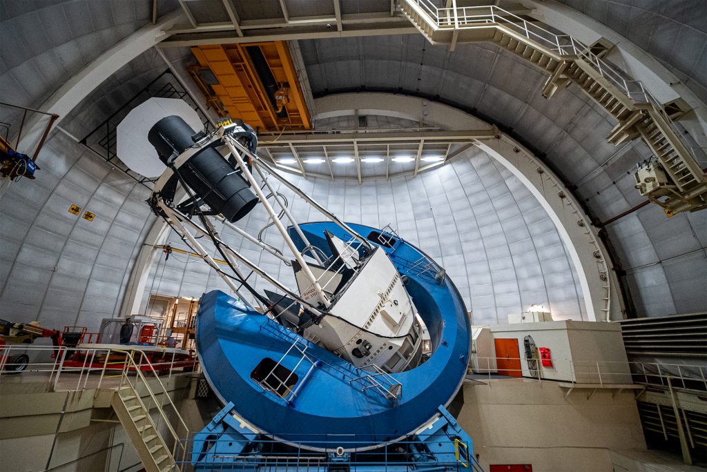
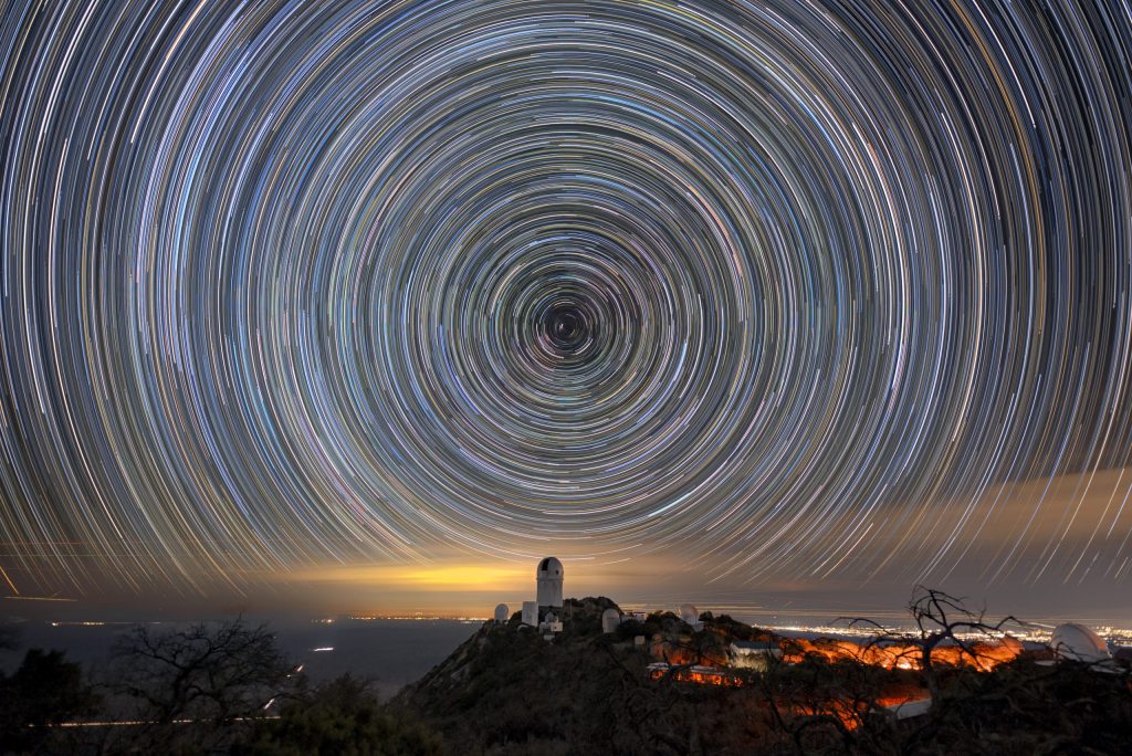
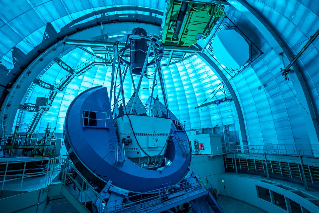
DESI is one of the most extensive surveys of the cosmos ever conducted. The state-of-the-art instrument, which capture light from 5,000 galaxies simultaneously, was constructed and is operated with funding from the DOE Office of Science. DESI is mounted on the U.S. National Science Foundation’s Nicholas U. Mayall 4-meter Telescope at Kitt Peak National Observatory (a program of NSF NOIRLab) in Arizona. The experiment is now in its fourth of five years surveying the sky, with plans to measure roughly 50 million galaxies and quasars (extremely distant yet bright objects with black holes at their cores) by the time the project ends.
Credit: Marilyn Sargent/Berkeley Lab
The new analysis uses data from the first three years of observations and includes nearly 15 million of the best measured galaxies and quasars. It’s a major leap forward, improving the experiment’s precision with a dataset that is more than double what was used in DESI’s first analysis, which also hinted at an evolving dark energy.
“It’s not just that the data continue to show a preference for evolving dark energy, but that the evidence is stronger now than it was,” said Seshadri Nadathur, professor at the University of Portsmouth and co-chair of DESI’s Galaxy and Quasar Clustering working group. “We’ve also performed many additional tests compared to the first year, and they’re making us confident that the results aren’t driven by some unknown effect in the data that we haven’t accounted for.”
DESI tracks dark energy’s influence by studying how matter is spread across the universe. Events in the very early universe left subtle patterns in how matter is distributed, a feature called baryon acoustic oscillations (BAO). That BAO pattern acts as a standard ruler, with its size at different times directly affected by how the universe was expanding. Measuring the ruler at different distances shows researchers the strength of dark energy throughout history. DESI’s precision with this approach is the best in the world.
“For a couple of decades, we’ve had this standard model of cosmology that is really impressive,” said Willem Elbers, a postdoctoral researcher at Durham University and co-chair of DESI’s Cosmological Parameter Estimation working group, which works out the numbers that describe our universe. “As our data are getting more and more precise, we’re finding potential cracks in the model and realizing we may need something new to explain all the results together.”
The collaboration will soon begin work on additional analyses to extract even more information from the current dataset, and DESI will continue collecting data. Other experiments coming online over the next several years will also provide complementary datasets for future analyses.
“Our results are fertile ground for our theory colleagues as they look at new and existing models, and we’re excited to see what they come up with,” said Michael Levi, DESI director and a scientist at Berkeley Lab. “Whatever the nature of dark energy is, it will shape the future of our universe. It’s pretty remarkable that we can look up at the sky with our telescopes and try to answer one of the biggest questions that humanity has ever asked.”
Videos discussing the experiment’s new analysis are available on the DESI YouTube channel. Alongside unveiling its latest dark energy results at the APS meeting today, the DESI collaboration also announced that its Data Release 1 (DR1) is now available for anyone to explore. With information on millions of celestial objects, the dataset will support a wide range of astrophysical research by others, in addition to DESI’s cosmology goals.
DESI is supported by the DOE Office of Science and by the National Energy Research Scientific Computing Center, a DOE Office of Science national user facility. Additional support for DESI is provided by the U.S. National Science Foundation; the Science and Technology Facilities Council of the United Kingdom; the Gordon and Betty Moore Foundation; the Heising-Simons Foundation; the French Alternative Energies and Atomic Energy Commission (CEA); the National Council of Humanities, Sciences, and Technologies of Mexico; the Ministry of Science and Innovation of Spain; and by the DESI member institutions.
The DESI collaboration is honored to be permitted to conduct scientific research on I’oligam Du’ag (Kitt Peak), a mountain with particular significance to the Tohono O’odham Nation.
Lawrence Berkeley National Laboratory (Berkeley Lab) is committed to groundbreaking research focused on discovery science and solutions for abundant and reliable energy supplies. The lab’s expertise spans materials, chemistry, physics, biology, earth and environmental science, mathematics, and computing. Researchers from around the world rely on the lab’s world-class scientific facilities for their own pioneering research. Founded in 1931 on the belief that the biggest problems are best addressed by teams, Berkeley Lab and its scientists have been recognized with 16 Nobel Prizes. Berkeley Lab is a multiprogram national laboratory managed by the University of California for the U.S. Department of Energy’s Office of Science.
DOE’s Office of Science is the single largest supporter of basic research in the physical sciences in the United States, and is working to address some of the most pressing challenges of our time. For more information, please visit energy.gov/science.
This press release was originally published by the U.S. Department of Energy’s Lawrence Berkeley National Laboratory. DOE’s Fermi National Accelerator Laboratory contributed key elements to DESI, including the online databases used for data acquisition and the software that ensures that each of the 5,000 robotic positioners are precisely pointing to their celestial targets to within a 10th of the width of a human hair.
Fermilab also contributed the atmospheric dispersion corrector, corrector barrel, hexapod and cage. The corrector barrel holds DESI’s six large lenses in precise alignment. The hexapod, designed and built with partners in Italy, focuses the DESI images by moving the barrel-lens system. Both the barrel and hexapod are housed in the cage, which provides the attachment to the telescope structure. In addition, Fermilab carried out the testing and packaging of DESI’s charge-coupled devices. The CCDs convert the light passing through the lenses from distant galaxies into digital information that can then be analyzed by the collaboration.
Key takeaways
- The Dark Energy Spectroscopic Instrument collaboration has publicly released the first 13 months of data from its main survey — a treasure trove that will help other researchers investigate big questions in astrophysics.
- Although DESI’s Data Release 1 is only a fraction of what the experiment will capture, the 270-terabyte dataset holds a vast amount of information, including precise distances to millions of galaxies.
- DESI’s data release contains more than twice as many unique objects outside our galaxy as in all previous 3D-spectroscopic surveys combined.
The Dark Energy Spectroscopic Instrument (DESI) is mapping millions of celestial objects to better understand dark energy: the mysterious driver of our universe’s accelerating expansion. Today, the DESI collaboration released a new collection of data for anyone in the world to investigate. The dataset is the largest of its kind, with information on 18.7 million objects: roughly 4 million stars, 13.1 million galaxies, and 1.6 million quasars (extremely bright but distant objects powered by supermassive black holes at their cores).
While the experiment’s main mission is illuminating dark energy, DESI’s Data Release 1 (DR1) could yield discoveries in other areas of astrophysics, such as the evolution of galaxies and black holes, the nature of dark matter, and the structure of the Milky Way.
“DR1 already gave the DESI collaboration hints that we might need to rethink our standard model of cosmology,” said Stephen Bailey, a scientist who leads data management for DESI and works at the U.S. Department of Energy’s Lawrence Berkeley National Laboratory (Berkeley Lab). “But these world-class datasets are also valuable for the rest of the astronomy community to test a huge wealth of other ideas, and we’re excited to see the breadth of research that will come out.”
DESI is an international experiment that brings together more than 900 researchers from over 70 institutions. The project is led by Berkeley Lab, and the instrument was constructed and is operated with funding from the DOE Office of Science. DESI is mounted on the U.S. National Science Foundation’s Nicholas U. Mayall 4-meter Telescope at Kitt Peak National Observatory (a program of NSF NOIRLab) in Arizona.
DESI’s data release is free and available to access through the National Energy Research Scientific Computing Center (NERSC), a facility at Berkeley Lab where DESI processes and stores data. Space fans can also explore some of DESI’s data through an interactive portal: the Legacy Survey Sky Browser.
The new dataset vastly expands DESI’s Early Data Release (EDR), containing roughly 10 times as much data and covering seven times the area of sky. DR1 includes information from the first year of the “main survey” collected between May 2021 and June 2022, as well as from the preceding five-month “survey validation” where researchers tested the experiment.
Objects in DESI’s catalog range from nearby stars in our own Milky Way to galaxies billions of light-years away. Because of the time it takes light to travel to Earth, looking out in space is akin to looking back in time. DESI lets us see our universe at different ages, from the present day to 11 billion years ago.
Although DR1 is just a fraction of what DESI will eventually produce, the 270-terabyte dataset represents a staggering amount of information, including precise distances to millions of galaxies. The release contains more than twice as many extragalactic objects (those found outside our galaxy) as have been collected in all previous 3D surveys combined.
Within its first year of operations, DESI became the single largest spectroscopic redshift survey ever conducted, sometimes capturing data on more than 1 million objects in a single month. For comparison, its predecessor, the Sloan Digital Sky Survey (SDSS), collected light from 9 million unique objects over roughly 25 years of operations. In 2024, DESI researchers used the data in DR1 to create the largest 3D map of our universe to date and make world-leading measurements of dark energy.
“The DESI project has maintained the pace of making 3D maps of the universe that are 10 times larger every decade,” said David Schlegel, one of the lead scientists at Berkeley Lab for both DESI and SDSS. “That’s our version of Moore’s Law for cosmology surveys. The rapid advance is powered by the clever combination of improved instrument designs, technologies, and analysis of ever-fainter galaxies.”
Large-scale science for a large-scale audience
DESI collects light from distant galaxies by using 5,000 fiber-optic “eyes.” Under clear observing conditions, the instrument can gather a new set of 5,000 objects roughly every 20 minutes, or more than 100,000 galaxies in one night. “DESI is unlike any other machine in terms of its ability to observe independent objects simultaneously,” said John Moustakas, a professor of physics at Siena College and co-lead of DR1.
The instrument separates the light from each galaxy into its spectrum of colors. This lets researchers determine how much the light has been “redshifted,” or stretched toward the red end of the spectrum by the universe’s expansion. Measuring the redshift of light from a distant object tells scientists how far away it is, meaning DESI can map the cosmos in three dimensions and reconstruct a detailed history of cosmic growth.
Every night, the images taken by DESI are automatically transferred to supercomputers at NERSC. The facility analyzes the data and sends them back to the researchers — a process they’re proud to advertise as “redshifts before breakfast.” This data transfer takes place via ESnet, the DOE’s dedicated high-speed network for science. The approach represents a new way of doing research where experimental facilities and data analysis are tightly coupled. This ecosystem forms an integrated research infrastructure that drastically accelerates the pace of science.
“For this data release, we made it so DESI could run on our most advanced supercomputer, Perlmutter,” said Daniel Margala, a scientific data architect at NERSC and part of the team that supports the DESI data processing. The transition to Perlmutter lets researchers take advantage of the supercomputer’s powerful GPUs (graphics processing units), processing the data nearly 40 times faster than was possible on previous NERSC systems. “What would have taken months on Cori [a prior-generation supercomputer] takes only weeks on Perlmutter.”
Even though they analyze data every night, researchers are always making improvements to their code to get the most possible information out of the light they collect. Once they hit a milestone, like collecting data for one year, they reprocess the full dataset with the best version of the code. It took about a month to crunch the DR1 dataset on Perlmutter.
That speed will be important as DESI collects even more data. The project is currently in its fourth of five years of data collection and aims to record spectra for more than 50 million galaxies and quasars before it ends.
Collaborators within DESI hope the experiment’s data will benefit researchers and enable those without access to large telescopes to advance their work. A major component of the data release is documentation to support other scientists, even those unfamiliar with the project, in understanding its contents.
“We’re still discovering all the things you can do with this dataset, and we want the community to be able to try out all their creative ideas,” said Anthony Kremin, a project scientist at Berkeley Lab who co-led processing of the new data release. “There are endless kinds of interesting science you can do when you combine our data with outside information.”
The DESI DR1 paper is available on the DESI Data website and will be posted on the online repository, arXiv. Videos discussing the data release are available on the DESI YouTube channel. Members of the collaboration presented the data release alongside DESI’s newest dark energy analysis in talks today at the American Physical Society’s Global Physics Summit in Anaheim, California.
DESI is supported by the DOE Office of Science and by the National Energy Research Scientific Computing Center, a DOE Office of Science national user facility. Additional support for DESI is provided by the U.S. National Science Foundation; the Science and Technology Facilities Council of the United Kingdom; the Gordon and Betty Moore Foundation; the Heising-Simons Foundation; the French Alternative Energies and Atomic Energy Commission (CEA); the National Council of Humanities, Sciences, and Technologies of Mexico; the Ministry of Science and Innovation of Spain; and by the DESI member institutions.
The DESI collaboration is honored to be permitted to conduct scientific research on I’oligam Du’ag (Kitt Peak), a mountain with particular significance to the Tohono O’odham Nation.
Lawrence Berkeley National Laboratory (Berkeley Lab) is committed to groundbreaking research focused on discovery science and solutions for abundant and reliable energy supplies. The lab’s expertise spans materials, chemistry, physics, biology, earth and environmental science, mathematics, and computing. Researchers from around the world rely on the lab’s world-class scientific facilities for their own pioneering research. Founded in 1931 on the belief that the biggest problems are best addressed by teams, Berkeley Lab and its scientists have been recognized with 16 Nobel Prizes. Berkeley Lab is a multiprogram national laboratory managed by the University of California for the U.S. Department of Energy’s Office of Science.
DOE’s Office of Science is the single largest supporter of basic research in the physical sciences in the United States, and is working to address some of the most pressing challenges of our time. For more information, please visit energy.gov/science.
Thirty years ago, the discovery of a long-sought particle was announced at the U.S. Department of Energy’s Fermi National Accelerator Laboratory by researchers with the Collider Detector at Fermilab experiment and the DZero experiment. This announcement marked the culmination of a worldwide hunt for the last quark predicted by the Standard Model.
CDF and DZero were both international scientific collaborations, each with about 450 researchers at the time of the top quark discovery. They included institutions from Brazil, Canada, Colombia, France, India, Italy, Japan, Korea, Mexico, Poland, Russia, Taiwan and the United States.
To mark the thirtieth anniversary of the top quark discovery at Fermilab, we spoke with two researchers who contributed to this breakthrough: Douglas Glenzinski, who worked on CDF, and Pushpalatha Bhat, who worked on DZero.
What is the top quark?
Bhat: “Once upon a time we thought atoms were the most elementary building blocks of matter. Then we discovered the nucleus, and its constituents: protons and neutrons. As we looked deeper and deeper into these particles, we found that they are made up of tinier particles called up and down quarks. Then we found out that there are other types of quarks, the strange quark and the charm quark. Fermilab then discovered the bottom quark in 1977. Once the fifth quark was discovered it was widely expected that there would be a sixth quark, the top quark, since quarks seem to come in pairs.”
Glenzinski: “The top quark is by far the heaviest of the quarks. It’s about the same mass as a gold atom, except this is a single quark. It was a little surprising that it was so much more massive than the other quarks.”
What are CDF and DZero?
Glenzinski: “CDF, or the Collider Detector at Fermilab, was one of the two international collaborations that operated at the Tevatron. CDF used a variety of technologies to measure the position, momentum and energy of particles created when protons and anti-protons from the Tevatron collided. The detector is about the size of a three-story house and looks like something out of a science fiction story.”
Bhat: “DZero was one of the two major collider experiments at the Tevatron. Its name comes from the interaction point in the Tevatron at which it’s located. These detectors are huge and have very complex detector subsystems, using different technologies and detection techniques.”
What were you working on in the CDF and DZero collaborations when the top quark was discovered?
Glenzinski: “When I joined CDF in 1992 as a graduate student, it was a very mature collaboration. The experiment had already been taking data for a long time and was in the middle of some upgrades. I was part of a team working on putting together a silicon microstrip vertex detector for the upgrade. CDF was the first to use this type of detector in a hadron collider. And the idea was that this upgrade would help reconstruct and study bottom quarks, which turned out to play an important role in the top quark discovery.”
Bhat: “As soon as I came to Fermilab in 1989, I joined DZero. At that time, we were putting the detector together, installing it and commissioning it. I took charge of the test beamlines and helped calibrate our calorimeters. Then we started taking data in late 1992. But finding this rare signal in data that had huge background events was like finding a needle in a haystack. I was in charge of the multivariate analysis group that used neural networks and other advanced techniques in top searches to discriminate against that background.”
Was there a specific moment when the collaborations knew they had the top quark?
Bhat: “On DZero, we were running data analysis from what was called the ‘express line’, with special events that had been filtered out from the whole data set and processed almost immediately. One event that came through the filter was striking. We calculated the probabilities that this was a top quark event using a multivariate method. And it was very highly likely. So that was the thing that made us go ‘Oh my God. We may be seeing the beginnings of top quark events!’ But we needed a significant number of top quark candidate events and careful estimates of background to be able to claim a discovery. With continued intense periods of data-taking and sophisticated analysis efforts by many people working relentlessly, we were able to do that.”
Glenzinski: “In CDF’s case, there had already been strong hints, and the collaboration published a paper in 1994 called ‘Evidence for top quark production,’ which was very suggestive but not statistically definitive. So, when data-taking resumed there was a lot of pressure to analyze the data as fast as we could. Many people worked to improve and update the analyses. And, as I remember it, there was a collaboration meeting where the updated results were unveiled. When it came time for questions, someone stood up and just said, ‘This is it, we did it. This is the top quark.’ The final result combined multiple analyses to get a more complete picture, and there was careful work to double-check everything with many people contributing, but, as I remember it, it was pretty clear to everyone what had happened.”
Looking back over the past 30 years, what has being part of this discovery meant?
Glenzinski: “It’s important to note that this was the result of collaboration-wide and lab-wide efforts over many years. It was extremely exhilarating to work in an international collaboration with a collection of people as motivated and bright as that. To have experienced that and had some impact on the top quark result just solidified my excitement for particle physics. I am grateful for having had that opportunity and for all those colleagues that mentored me, and the other graduate students involved.”
Bhat: “Being part of the top quark discovery (and then the Higgs boson) has been incredible. The top quark is very special. Because it’s so heavy, it’s the quark that couples very strongly to the Higgs boson which helps us understand the electroweak theory and symmetry breaking better. Together with the Higgs boson, the top quark also has implications for the stability of the universe.”
Fermi National Accelerator Laboratory is America’s premier national laboratory for particle physics and accelerator research. Fermi Forward Discovery Group manages Fermilab for the U.S. Department of Energy Office of Science. Visit Fermilab’s website at www.fnal.gov and follow us on social media.