What do you do at Fermilab?
I’m an associate scientist and the group leader of the Materials for Quantum Devices group within the Superconducting Quantum Materials and Systems Division at Fermilab, part of the Department of Energy’s National Quantum Information Science Research Center — SQMS. The research group primarily focuses on improving the length of time information can be effectively stored and processed in a superconducting quantum device. Dramatically extending this coherence time is critical for realizing next-generation quantum computers and sensors.

Akshay Murthy is an associate scientist and group leader at SQMS, as well as an avid runner.
Our group is composed of graduate students, postdoctoral researchers and engineers. We collaborate to improve coherence times by applying a variety of advanced materials characterization tools — electron microscopy, X-ray photoelectron spectroscopy and time-of-flight secondary ion mass spectrometry — to understand the physical processes that lead to the loss of quantum information, called decoherence. We aim to answer questions such as:
- Are the surfaces of these materials ordered or disordered? What about the interfaces between materials?
- What impurities are present in our materials? Where are they located?
- What types of defects are present in these devices? How do they respond during device operation at cryogenic temperatures?
Using these techniques as part of a materials-oriented approach, the SQMS research team has recently achieved leading coherence times in transmon qubits.
I’m also the leader for the materials for 2D and 3D quantum devices focus area in the SQMS center, which consists of over 70 researchers across 11 partner institutions focused on fabrication of quantum devices, as well as characterization of quantum devices using structural, chemical, superconducting and microwave-based methods. In this role I prioritize, manage and evaluate activities to ensure SQMS achieves its research goals in a timely fashion. I am extremely passionate about advancing the performance of superconducting qubit platforms, with my ultimate goal being to help deliver a transformational new paradigm in computing. Solving critical scientific and engineering challenges in this field requires the type of coordinated ecosystem involving academic institutions, national labs and industry partners, which we have created as part of SQMS. I am proud of the advances our center has already demonstrated and expect many exciting new achievements in the years to come.
How long have you worked at Fermilab?
I have worked at Fermilab for almost four years now. I was initially hired as a postdoctoral research associate in the SQMS division before being promoted to associate scientist. Throughout this time, I have had the wonderful opportunity to work alongside a variety of world-leading scientists and engineers, both at Fermilab and at SQMS partner institutions, in a wide variety of areas, including accelerator physics, quantum physics, materials science, microwave engineering, nanofabrication and beyond. Prior to joining Fermilab, I completed my Ph.D. at Northwestern University in the group of Professor Vinayak Dravid and worked in industry.
What is the most challenging part of your work?
Understanding what limits the lifetime of quantum states in superconducting qubits is without question what I find to be the most challenging part of my work. These quantum devices are exceedingly sensitive and understanding the complex interplay between defects, impurities, interfaces and surfaces on various performance metrics presents an imposing challenge daily.
What is the most rewarding part of the work you do at Fermilab?
Developing a hypothesis and testing it through a series of systematic experiments is the most rewarding part of my work. No matter whether the original hypothesis is supported by the investigation or whether it requires refining, every experiment serves as an opportunity to learn something new. It’s this opportunity to continuously acquire new knowledge that excites me to come to work every day.
What do you do for fun outside of work?
I’m an avid long-distance runner and have run over a dozen half marathon and marathon races, including the Chicago Marathon and Boston Marathon. You can usually find me Saturday mornings running along the lakefront or on the Illinois Prairie Path. I enjoy experiencing the beauty and sounds that nature has to offer while simultaneously pushing my body to its limits.
Fermi National Accelerator Laboratory is supported by the Office of Science of the U.S. Department of Energy. The Office of Science is the single largest supporter of basic research in the physical sciences in the United States and is working to address some of the most pressing challenges of our time. For more information, please visit science.energy.gov.
Teams from Fermi National Accelerator Laboratory and Sanford Underground Research Facility have successfully completed the first test lift and lowering of a six-ton L-shaped steel beam for construction of the Deep Underground Neutrino Experiment in Lead, South Dakota.
Transporting a large, irregularly shaped steel component down a narrow mine shaft into a cavern a mile underground at SURF is not an easy task due the size and weight of the beam and the elevator-like cargo space about the size of a backyard storage shed. The successful test is a significant step forward, allowing engineers and crews to anticipate future challenges.
DUNE is an international collaboration, and the steel components are an in-kind contribution to the experiment by CERN. The initial overseas shipment of beams earlier this year is just the beginning of the 2,100 structural elements that will be delivered to SURF early next year.
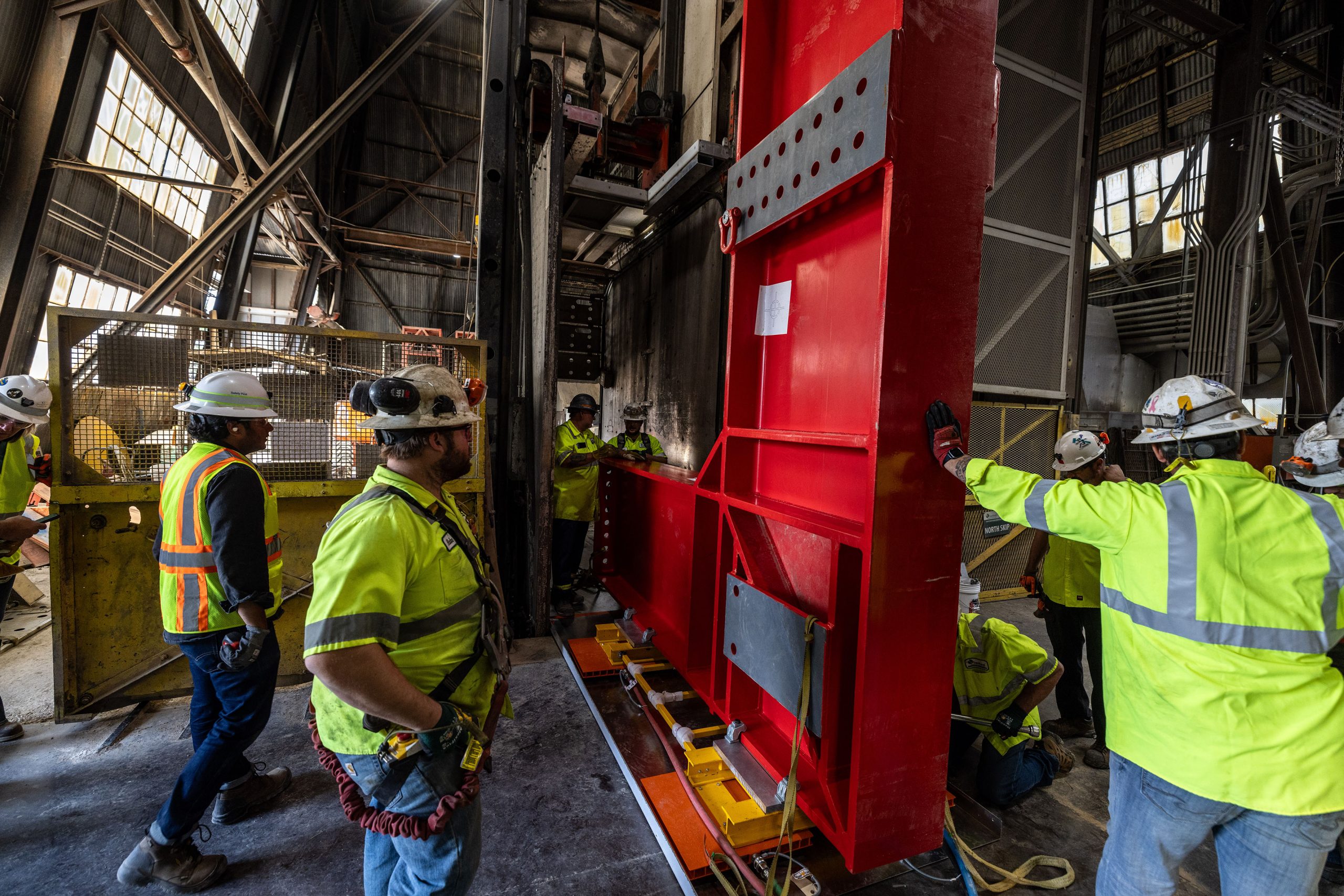
Supported from above by a crane, the L-beam is carefully moved into position by the rigging team for transport down the mine shaft in Lead, South Dakota. Photo: Matthew Kapust, SURF
“Our entire team was excited to see the steel arrive in South Dakota for testing,” said Jolie Macier, far detector and cryogenics project manager with Fermilab. “I’m grateful for everyone from SURF who helped in this year-long planning process, as well as our partners from CERN. This is truly a collaborative effort.”
The first two beams, delivered in January, are part of the external structure for DUNE’s massive cryogenic vessels in the Long-Baseline Neutrino Facility. Once assembled with the other 2,500 tons of steel, they will help form a structure measuring 216 feet long, 62 feet wide and 60 feet high. After the internal insulating material is installed, the integrated structure will support and house a particle detector that will be filled with 17,000 tons of liquid argon cooled to minus 302 degrees Fahrenheit (minus 186 degrees Celsius). Scientists will use these detector modules in the quest to understand neutrinos — ghostly particles that are incredibly challenging to detect.
No surprises
Months of careful planning among the LBNF/DUNE international partners paved the way for this first success.
“We don’t want any surprises when we’re lifting heavy steel items into the shaft,” said Jeff Barthel, rigging supervisor at SURF. “You learn things when testing and this testing helped identify steps that can be taken to make this a safe and repeatable task when the time comes to lower the large numbers of cryostat components necessary for the Far Site Detectors.”
This test involved one of the many steel L-shaped beams that will form the corners of the structure. Due to their size, shape and center of gravity, the L-beams present some unique constraints. The initial L-beam lowered in this test measures about 18 feet long and 12 feet wide and weighs 12,000 pounds.
“The most critical thing for the L-beam is the tipping angle, because the tilt can’t be more than five degrees,” said Sanmitra Pingulkar, a mechanical engineer with Fermilab. “The beam had to fit within the footprint of the cage and the shaft, and crews also had to keep in mind the weight of the total load could not exceed 13,500 pounds. 90% of the weight for this particular lift was the L-beam itself.”
As the beam reached the bottom of the elevator shaft after its 100 feet-per-minute descent nearly a mile underground, crews were rewarded for their diligent planning.
“In the end the L-beam was stable and stayed within one degree. It was a success,” said Pingulkar.
“And the success of this test is thanks to a collaborative effort from everyone involved over the past year of planning,” added Charles Maupin, a mechanical engineer with SURF. “This learning experience marks the first of many pieces of cryostat steel we will transport 4,850 feet underground at SURF.
Perfecting procedures
To prepare for the test lift of a steel beam, crews at SURF first created a full-scale wooden replica of an L-beam last spring. While much lighter than the actual steel component, the shape and center of gravity of the mockup helped create a better understanding of how crews could most effectively handle the steel structures.
For the LBNF/DUNE project alone, SURF performed 350 lifts to this point. This work includes analyzing load dynamics and limitations of the rigging equipment, as well as minimizing risk for unexpected occurrences, such as the cage coming to a sudden stop in the shaft.
“You have to quantify everything,” Barthel said. “If something happens, operations could be shut down for a long time. It could have huge ramifications that cost the project months. You cannot take a chance with any of that.”
“There are a lot of people that put a lot of effort and thought into these lifts,” Barthel added. “The professionalism and teamwork shown by our crew members during the test lift was a testament to their training and skill.”
In late 2022, CERN, in collaboration with Fermilab and SURF, successfully conducted a similar test for large, fragile DUNE particle detector components known as anode plane assemblies.
International partnership
Members of CERN were onsite at SURF during the execution of the lift. Olga Beltramello, a CERN mechanical engineer, was one of the observers present at SURF for the lowering test.
“This test was an important learning opportunity,” said Beltramello. “It’s very important for CERN, not only that we check that everything works, but also that the timing of the lowering of the equipment is compatible with the rest of the installation schedule for the cryostat delivered by CERN.”
“Our partnership with CERN is an important element of the LBNF/DUNE project,” added Macier. “Their commitment to the success of this collaboration is critical and much appreciated.”
A step closer
The successful test for lowering the heavy steel components brings the international collaboration a significant step closer to the start of the DUNE detector installation. Once operational, a beam of neutrinos sent from Fermilab’s campus near Chicago will travel 800 miles through the earth to DUNE’s massive underground detectors at SURF. Scientists expect DUNE to paint a clearer picture of how neutrinos behave and transform into various states, and even provide clues for the origin of matter in the universe
More than 1,400 scientists and engineers in over 35 countries are contributing to the experiment.
Fermi National Accelerator Laboratory and Sanford Underground Research Facility are supported by the Office of Science of the U.S. Department of Energy. The Office of Science is the single largest supporter of basic research in the physical sciences in the United States and is working to address some of the most pressing challenges of our time. For more information, please visit science.energy.gov.
Sanford Underground Research Facility is operated by the South Dakota Science and Technology Authority (SDSTA) with funding from the Department of Energy’s Office of Science. We are America’s Underground Lab. Our mission is to advance world-class science and inspire learning across generations. Visit SURF at www.sanfordlab.org.