Researchers from the U.S. Department of Energy’s Fermi National Accelerator Laboratory are experts in making microelectronics and data processing more efficient and powerful. This collective knowledge comes from decades of developing giant detectors for high-energy physics.
On July 17, two distinguished guests joined researchers at Fermilab to sign the Energy Efficiency Scaling for 2 Decades pledge, or EES2. These guests include Tina Kaarsberg, a program manager from the DOE’s Office of Energy Efficiency and Renewable Energy; and Sadasivan Shankar, research technical manager from DOE’s SLAC National Accelerator Laboratory.
“Fermilab has emerging core competencies in circuits, architectures and edge algorithms,” said Lia Merminga, Fermilab’s director. “Our lab has been designing low-power circuit solutions for advanced scientific instrumentation, detectors, accelerators and more for four decades.”
The EES2 pledge
Since the 1940s, computational power has grown exponentially. This growth has largely been sustained according to Moore’s law, which observes the number of components per integrated circuit doubling every year. But current computing technologies are not efficient enough to meet society’s demands to produce and process more data.
Fermilab has become the 48th organization to sign the EES2 pledge. The EES2 pledge seeks to improve the efficiency of electronics and support American manufacturing. Led by the DOE’s Advanced Materials and Manufacturing Office, this pledge aims to set the semiconductor industry on the path to double energy efficiency every two years. It also looks to increase the competitiveness of semiconductor manufacturers and strengthen clean energy supply chains in America.
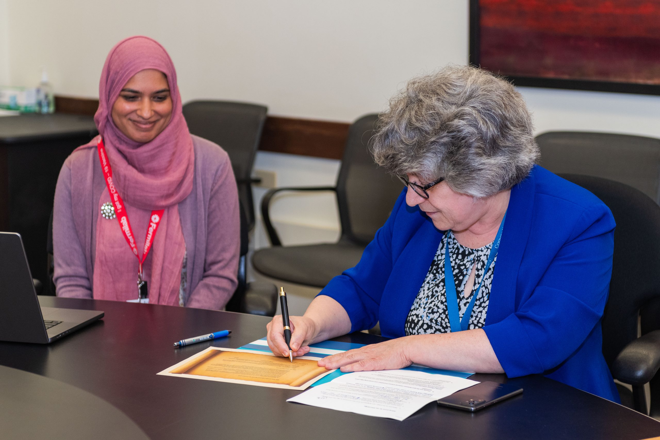
Farah Fahim, the division head for Fermilab’s Microelectronics Division (left) and Lia Merminga, Fermilab’s director, sign the EES2 pledge. Photo: Ryan Postel, Fermilab
To meet this goal, four working groups will participate in EES2 workshops and contribute a roadmap.
“This EES2 pledge is a win for the environment without compromising science,” said Shankar. “Technological innovations are needed to enable this paradigm of energy-efficient computing since more and more energy is spent on analyzing data. Fermilab can play an invaluable role in extending the premise of intelligent sensing to applications beyond particle detectors.”
Fermilab’s emerging technologies
During the visit, guests toured Fermilab’s facilities to see how the lab strives to improve efficiency in computing and detectors. At the start of the tour, visitors listened to talks about driving innovation.
Researchers demonstrated a few ways AI-on-chip is used to advance Fermilab’s mission. They shared how an artificial intelligence algorithm compresses data for the Compact Muon Solenoid at the CERN Large Hadron Collider. They showed how researchers test and analyze electronics using robotics. The researchers presented advanced 3D chips and investigations with industry to improve devices. They also discussed collaborating on open-source platforms to develop and test solutions in AI.
“Designing and developing energy-efficient detectors with integrated sensing, computing and communications over the next several years will create impactful hardware for the next generation of high-energy physics experiments and beyond,” said Farah Fahim, the division director for Fermilab’s Microelectronics Division.
Next, guests toured the new, sustainably built Integrated Engineering Research Center. Nicola Bacchetta, a senior scientist at Fermilab, explained how this space will help engineers develop and assemble particle detectors.
Researchers from the Fermilab Quantum NETwork presented a network to share quantum information across the Chicago region. This network includes Argonne National Laboratory and Northwestern University’s campuses in Evanston, Illinois, and Chicago.
The tour ended at Fermilab’s Silicon Detector building where the group saw firsthand how Fermilab researchers build, package, test and characterize detectors for experiments.
“Energy efficiency is aligned with the strategy of our laboratory, and microelectronics is only part of it,” said Merminga. “We plan to develop a strategy for sustainability in our laboratory that expands over scientific infrastructure, accelerators, buildings, detectors and microelectronics. Signing this pledge is the right thing to do for our society; it is well aligned with our principles, and we bring unique capabilities to this important cause.”
Fermi National Accelerator Laboratory is supported by the Office of Science of the U.S. Department of Energy. The Office of Science is the single largest supporter of basic research in the physical sciences in the United States and is working to address some of the most pressing challenges of our time. For more information, please visit science.energy.gov.
Recommended reading
Using AI, Fermilab researcher probes how transistors behave in extreme cold
Olivia Seidel’s work draws on Fermilab’s deep expertise in microelectronics and cryogenic devices to support key goals of the Genesis Mission — a sweeping U.S. Department of Energy artificial intelligence initiative.
Fermilab leads multi-lab AI initiative to accelerate design of chips used in extreme environments
Researchers with Department of Energy national laboratories are working together alongside industry collaborators to support Genesis Mission goals by using the power of artificial intelligence to significantly reduce design times of custom computer chips for use in extreme temperature, high-radiation and ultra-fast environments.
New electronically tunable quantum detector speeds up search for dark matter
Scientists designed a state-of-the-art detector to electronically tune itself, enabling scientists to search broader frequency ranges for evidence of weak signals produced by dark photons — possible dark matter particles — much faster and more precisely than ever before.