
Olivia Seidel is tackling a problem that sounds deceptively simple: understanding how transistors behave when they get very cold. The answers she finds could shape everything from quantum computers to satellites in outer space, and she is using artificial intelligence to accelerate that research.
A Ph.D. student working within Fermi National Acceleratory Laboratory’s Microelectronics group, Seidel is leveraging AI for cryogenic transistor modeling. Her work draws on Fermilab’s deep expertise in microelectronics and cryogenic devices to support key goals of the Genesis Mission — a sweeping national AI initiative combining the expertise of the Department of Energy’s national laboratories, U.S. research universities and industry to supercharge American innovation.
I recently visited Seidel at her office in Fermilab’s iconic Wilson Hall to talk about the exciting work underway.
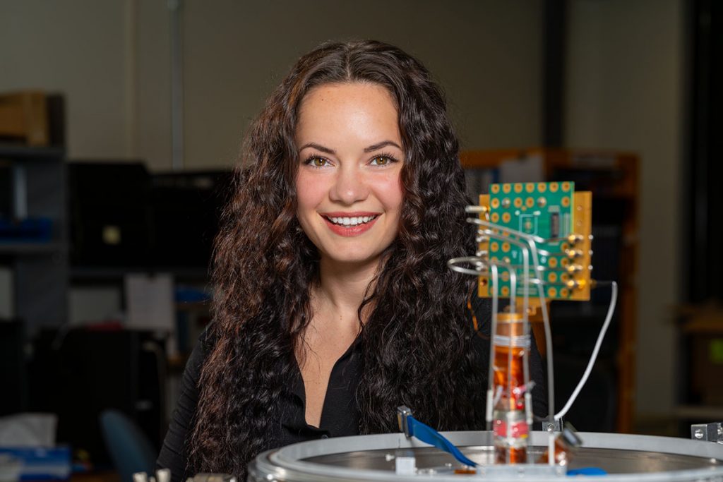
Q: What exactly is a transistor, and why should anyone care about how it behaves in the cold?
Transistors are the computational building blocks of every electronic device you use — your phone, your laptop, anything that manipulates bits and bytes. Over decades, industry has become extraordinarily good at making them smaller and more powerful. We’re talking about transistors just a few nanometers across — so small that a single wavelength of visible light is hundreds of times wider.
For most of that history, room temperature was the only environment that mattered. But quantum computing and other emerging technologies require electronics that function at cryogenic temperatures — just a few degrees above absolute zero. And at those extremes, transistors behave very differently.
Q: How do the transistors behave differently?
One of the clearest examples is what it takes to switch a transistor on. At room temperature, you apply a certain voltage, and it turns on. At deep cryogenic temperatures below 4 kelvin [about minus 452 degrees Fahrenheit], like the temperatures of outer space, it takes significantly higher voltage to flip that switch. The whole curve of the transistor’s behavior shifts.
That might sound like a minor technical detail, but if you’re a circuit designer unaware of that shift, your entire circuit can fail. It could also technically work while consuming far more power than it should — and in a cryogenic environment, excess power means excess heat, which can be catastrophic. Heat causes decoherence in quantum systems, essentially causing quantum properties to fall apart, and can disrupt electronics trying to detect neutrinos in a cryogenic liquid-argon environment.
Q: Do you build the models that predict this behavior?
I do! I build physics models that accurately describe how transistors behave at cryogenic temperatures, and we measure transistors in the lab at those temperatures to inform and validate the models. The goal is that when a circuit designer sits down to build something that needs to operate at 4 kelvin, they can trust the model — rather than building the whole thing, putting it in a cryogenic system and finding out it doesn’t work.
Q: What are some of the real-world applications that would benefit from this knowledge?
There are several. One big area is trapped ion quantum computing. Ions — charged atoms — can serve as qubits, and to manipulate them precisely, you use high-voltage transistors in an extremely cold environment. The cold suppresses thermal noise, helping preserve the fragile quantum state of the qubit.
Another application is superconducting nanowire single-photon detectors, or SNSPDs — thin superconducting films that detect single particles of light. These are used for particle detection and precision measurements and also require electronics that function at deep cryogenic temperatures.
There’s also interest in using cryogenic transistors for the readout and control of superconducting qubits — having electronics that live inside the cryogenic system itself rather than sending signals back up to room temperature. Along with quantum applications, there are particle physics uses at Fermilab, like the large liquid-argon detectors in the DUNE at LBNF neutrino experiment, and interest from deep space satellite designers where the background temperature of the universe sits around 3 kelvin [about minus 454 degrees Fahrenheit].
Q: That’s a wide range of applications. How long does it currently take to build these models?
That’s the problem. Using standard industry tools, building a robust set of cryogenic physics models for one type of transistor can take around two years. Technology advances faster than the models do — and that’s an industry-wide challenge.
Q: Is this where AI and machine learning can come in?
Through the Genesis Mission, DOE is harnessing capabilities at the national laboratories by using AI to make laborious, data-rich research processes dramatically faster. Our work on cryogenic transistor modeling is a direct example.
The idea is to use machine learning to speed up the modeling process enormously. Instead of painstakingly fitting physical parameters using other tools, we let the AI/ML model directly predict the model from the measurement data we collect in the lab.
As a proof of concept, I built a prototype that replaces one step in the traditional modeling process with a machine learning approach, yielding results just as good, if not better, than the conventional method.
The key metric is the time required to go from an undefined set of physics-model parameters to a complete, working parameter set tailored to a given transistor and capable of accurately predicting its deep-cryogenic behavior.
“We’re laying the groundwork so that future researchers don’t have to spend years on something a well-trained model can do in a fraction of the time.”
Olivia Seidel
Using the new machine learning approach, I spent roughly two weeks generating training data and building the model. Once trained, it predicts optimal physics parameters from deep cryogenic transistor measurement data in approximately 120 milliseconds. The conventional approach, by contrast, can take anywhere from weeks to months, depending on the transistor.
That prototype is a core aspect of the Accelerating eXtreme Environment Specs-to-Silicon project led by Fermilab — a Genesis Mission initiative advancing microelectronics in extreme environments where industry expertise and investment remain scarce. We’re using my work to build a complete deep cryogenic model for transistors highly sought after for quantum information science and high energy physics applications at 4 kelvin. The goal is a full, production-quality model built from the ground up using AI — not just adapting a room-temperature model and hoping it holds at cryogenic temperatures.
Q: What does “from the ground up” mean in this context?
Currently, the standard approach is to take a room-temperature transistor model and adapt it to cryogenic temperatures, re-extracting all the physics parameters to fit what you actually measure. It works, but it’s slow and laborious.
The longer-term vision is to build models starting from the material properties of the transistor itself — not from a room-temperature approximation. The machine learning model would infer the underlying physics directly from lab measurements, rather than adjusting a pre-existing framework. It’s a fundamentally different and more powerful approach.
Q: What do you think about the significance of this work within the broader picture?
Cryogenic transistor modeling was something that wasn’t at the forefront of our thinking about twenty years ago. Now it’s increasingly critical infrastructure for quantum computing, particle physics and space technology — and the demand is only going to grow.
What we’re doing with machine learning is similar to how Fermilab once automated wire bonding — a precise, painstaking manual process of connecting tiny wires to chips by hand. Eventually machines took over, freeing skilled people to focus on harder problems. We’re laying the groundwork so that future researchers don’t have to spend years on something a well-trained model can do in a fraction of the time. It’s not replacing the science — it’s making the science move faster.
Fermi National Accelerator Laboratory is America’s national laboratory for particle physics and accelerator research. Fermi Forward Discovery Group manages Fermilab for the U.S. Department of Energy Office of Science. Visit Fermilab’s website at www.fnal.gov and follow us on social media.
Recommended reading
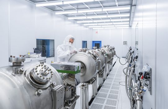
DOE selects Fermilab-led AI initiative to advance particle accelerator performance
In a project selected for funding by the Department of Energy’s Genesis Mission, Fermi National Accelerator Laboratory and partners from other national laboratories, universities and industry will apply artificial intelligence and machine learning to enable precise and adaptive resonance control in particle accelerators. Their work aims to lower operating costs by millions of dollars each year and improve accelerator performance, driving scientific discovery.
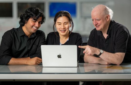
DUNE uses AI to transform the future of neutrino research
DUNE is pioneering the future of neutrino research by integrating artificial intelligence into its experiment, drawing on decades of machine learning work at Fermilab.

U.S. Department of Energy invests in Fermilab projects to accelerate AI-enabled scientific discovery
The awards will support Fermilab projects by leveraging AI to boost innovation and technology development, advance DOE’s Genesis Mission and accelerate scientific discovery.