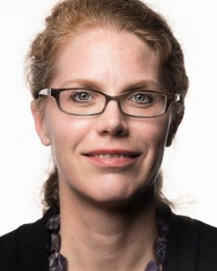
The U.S. Department of Energy’s Fermi National Accelerator Laboratory welcomes Greg Stephens as the lab’s new chief operating officer beginning May 6, 2024.
Stephens brings more than 35 years of experience in commercial, academic, international and U.S. government operations, working in project management, business administration, environment, safety and health, and engineering. He has served at 11 of the 17 U.S. national laboratories. At each lab, Stephens took on a wide array of roles including project and program manager, chief engineer, chief information officer, chief technical officer and operations director.
“We are delighted to have Greg Stephens join Fermilab in leading the operation of the lab,” said Fermilab Director Lia Merminga. “His extensive experience, including at many of the national laboratories, and leadership roles, will be a huge asset in his leadership of our laboratory operations toward the safe, secure, efficient and effective execution of our mission.”
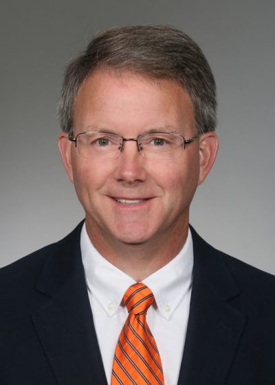
Fermilab welcomed Greg Stephens as the lab’s new chief operating officer on May 6, 2024. Photo: Amentu
Most recently, Stephens was vice president for Amentum’s Technical Services. Here he led a diverse staff that delivered operations, engineering, maintenance, safety, quality assurance, risk assessment, business and project optimization, and management services.
Under his leadership, the division supported a wide array of high-hazard chemical, biological and nuclear operations customers from around the world, including U.S. and international laboratories, research and development entities, commercial companies and emergency preparedness institutions.
“I am excited and honored to join the Fermilab team, the premier particle physics laboratory in the U.S.,” Stephens said. “I look forward to collaborating with the talented Fermilab employees to drive innovation and continue the excellent scientific research. I believe there is an exciting future at Fermilab and look forward to bringing my passion and expertise to this team as we capture the opportunities ahead.”
Stephens is an electrical engineer with a degree from Clemson University. He began his career with DuPont de Nemours, Inc. in the Engineering Services Division and with General Electric in the Simulation and Space Systems Manufacturing Management Program. He also had numerous project and program management assignments at Westinghouse, Washington Group International, URS, AECOM and Amentum.
Stephens has served on the Board of Directors for Helping Hands of Aiken and the United Way of Aiken County while also on the Engineering Advisory Board for the University of South Carolina at Aiken. He and his wife Jane have three grown children and one grandchild.
Fermi National Accelerator Laboratory is supported by the Office of Science of the U.S. Department of Energy. The Office of Science is the single largest supporter of basic research in the physical sciences in the United States and is working to address some of the most pressing challenges of our time. For more information, please visit science.energy.gov.
By R.E. Natowicz
Cutting-edge particle physics research is always in season at Fermi National Accelerator Laboratory, but spring is a most special time of the year as Fermilab’s baby bison are born. Today, two bison calves were born, marking the start of calving season at Fermilab.
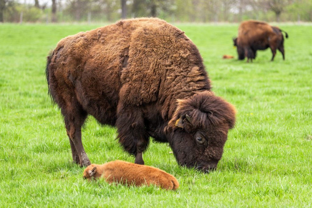
Bison season has started at Fermilab with the birth of not one, but two bison calves arriving today! You can visit the bison as Fermilab is open from dawn to dusk every day of the week. Photo: Dan Svoboda Fermilab
Cleo Garcia, a member of the Grounds Maintenance team who has the important job of caring for the bison herd, said that during this season Fermilab is expecting the births of about 20 calves.
Garcia gives extra attention to the female bison, called cows, to estimate the number of new births to expect each year. He watches for physical changes and considers the age of the cows to make this determination.
The Fermilab herd currently consists of 24 cows and two bulls. “Some of them are getting older and might not calve this year,” Garcia said. Last year the cows gave birth to 20 calves, and in the year prior there were 21 births.
In addition to contributing to the conservation of American bison, Fermilab’s herd is a huge draw for visitors. “They’re big animals, and visitors bring their kids who enjoy watching them,” Garcia said.
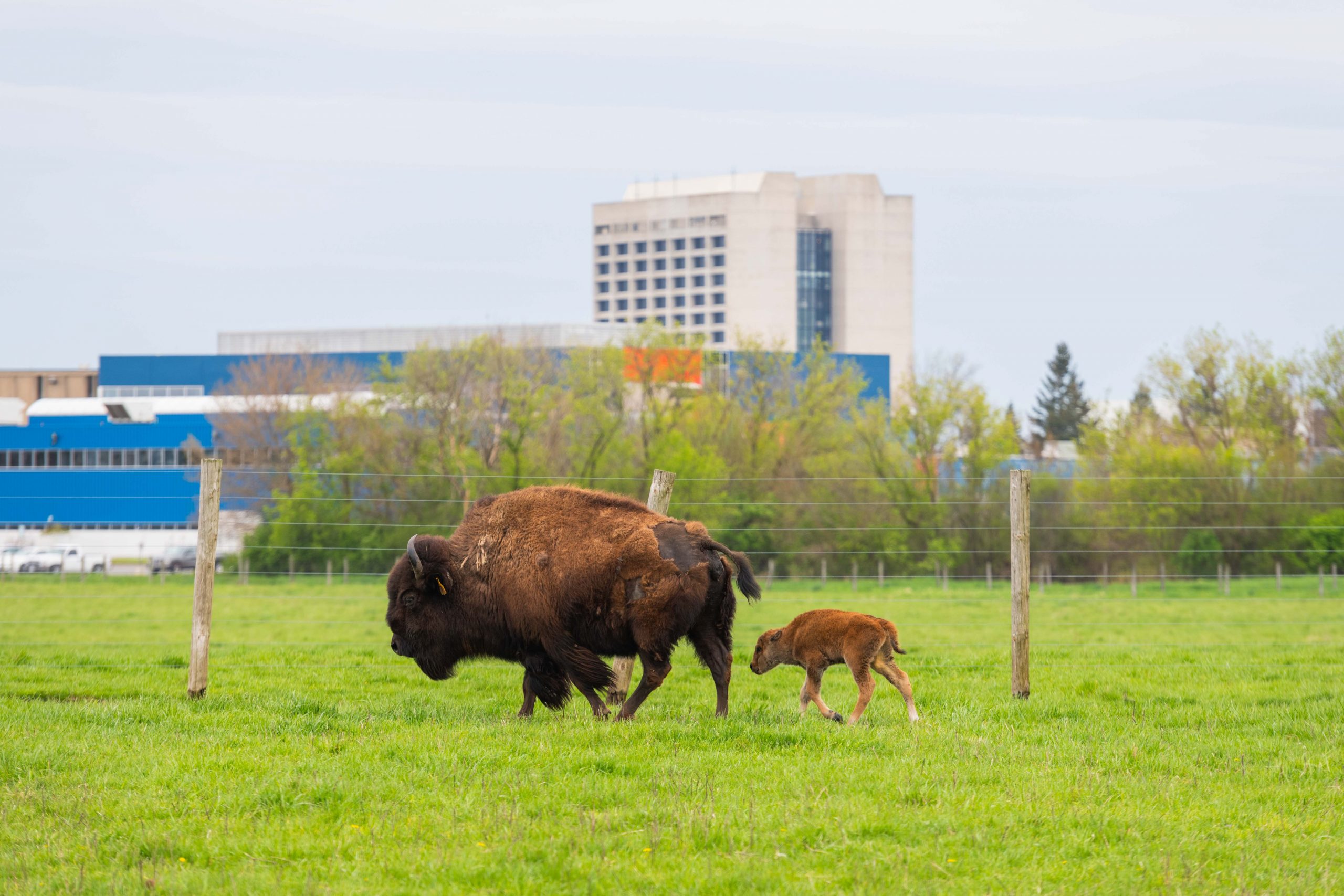
Photo Ryan Postel, Fermilab
Garcia notes that the bison have their own personalities — some being more docile, some wilder. They play and engage with each other in different ways. Sometimes the bulls will charge at each other. Most importantly, the bison are very protective of their small calves.
The lab’s first director, Robert R. Wilson, pioneered the idea of making bison a Fermilab tradition. He wanted to show that Fermilab was on the frontier of particle physics research, and bison represented the frontier era. “When you’re outside with them, you’d think you’re out in the prairie,” Garcia said.
Bison are sizable animals: the bulls can weigh over one ton, and cows average between 900 and a little over 1000 pounds. When calves are born, they weigh between 40-70 pounds. The calves grow quickly — just six months later they usually have grown to between 300 and 350 pounds. When bison babies are first born, they are cinnamon colored, and two months later their fur deepens to a darker shade of brown.
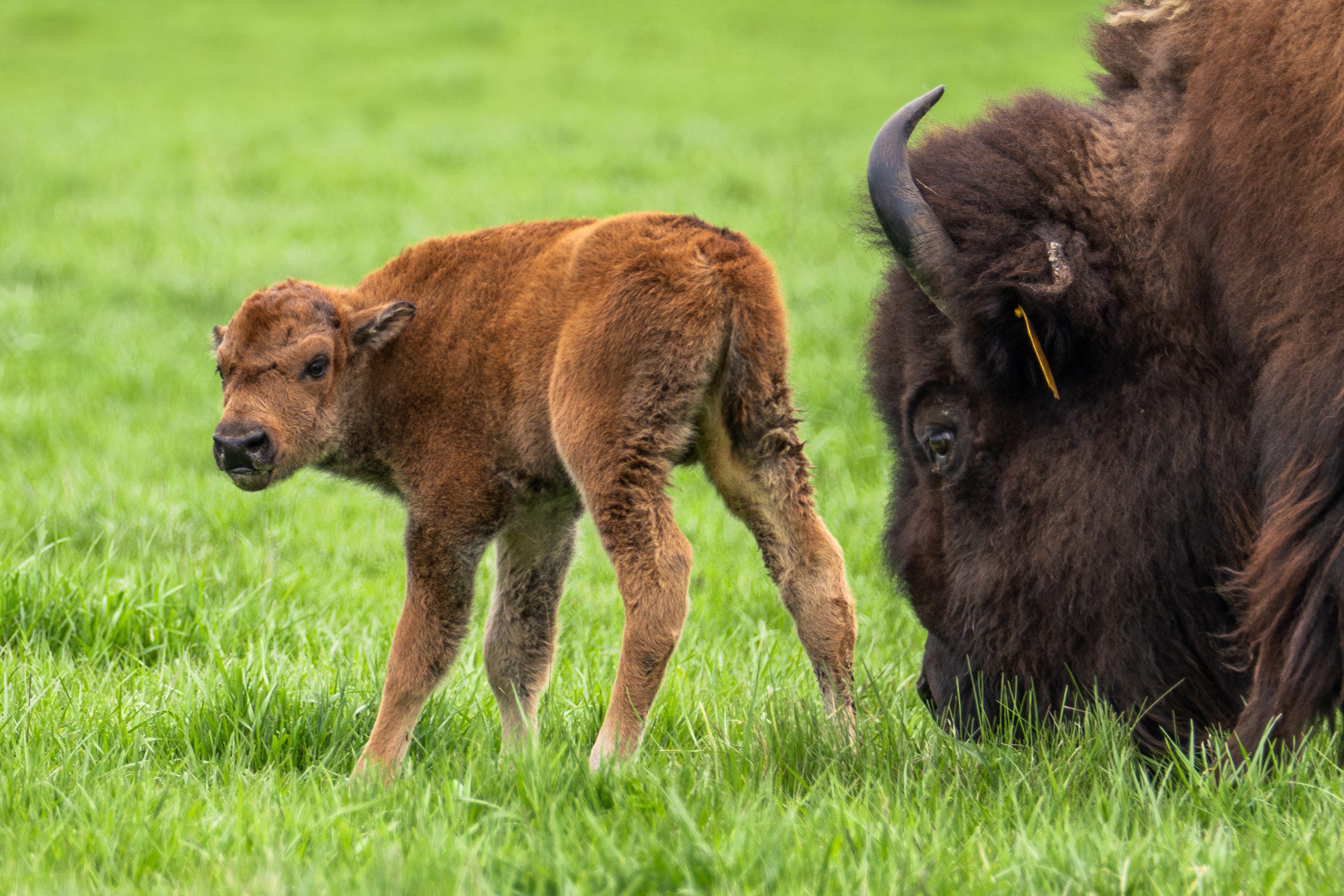
Photo: Dan Svoboda Fermilab
Fermilab refreshes the bulls in the herd every five to seven years. The Fermilab bulls have been genetically tested to ensure that they are pure-bred American bison. This is key to maintaining the health of the herd. In 2015, Fermilab tested the entire herd and determined that there were no domesticated cattle genes present.
Calving season usually starts in the middle of April and continues until June. Although there are signs of an early spring in Illinois this year, Garcia noted that so far he hasn’t seen indications that warmer weather is affecting the herd, but added, “We’ll see how the season goes.”
Bison are hardy animals that can live outside year-round in most any weather. Even so, their Fermilab keepers provide them with structures within the corrals to block the wind that can whip across Fermilab’s flat prairie land.
As part of his duties, Garcia feeds the bison and checks on their well-being daily — especially during calving season. He visits all the cows to watch for signs that they may soon give birth. Garcia also monitors the young calves to make sure that they are healthy. During the winter he supplements the herd’s food with hay and grain. Visitors in the summer will see the bison grazing upon plentiful grasses naturally growing on Fermilab’s grounds. They only need to be given ample water during these months.
Garcia said he likes being outdoors with the animals. “Calving season is the most rewarding time of the year,” he said. “You see new life coming to the land.”
You can view the bison herd anytime from the bison camera or visit Fermilab seven days a week during outdoor visiting hours from dawn to dusk.
The Fermilab site has been designated a National Environmental Research Park by the U.S. Department of Energy. The lab’s environmental stewardship efforts are supported by the Department of Energy Office of Science as well as Fermilab Natural Areas.
Fermilab is supported by the Office of Science of the U.S. Department of Energy. The Office of Science is the single largest supporter of basic research in the physical sciences in the United States and is working to address some of the most pressing challenges of our time. For more information, visit Fermilab’s website and follow us on Twitter at @Fermilab.
Bonnie Fleming, the chief research officer at the U.S. Department of Energy’s Fermi National Accelerator Laboratory, was elected as a member of the American Academy of Arts & Sciences in Mathematical and Physical Sciences. As chief research officer, Fleming leads all areas of science and technology at Fermilab.
Bonnie Fleming is a 2024 member of the prestigious American Academy of Arts & Sciences. Photo: Reidar Hahn, Fermilab
Fleming has made significant contributions to neutrino research by pioneering a class of detectors called Liquid Argon Time Projection Chambers. This technology provided a giant leap forward in how scientists may study the varying states of neutrinos and how the subatomic particles might interact with matter. These detectors are the core to Fermilab’s neutrino experiments, including the future international Deep Underground Neutrino Experiment.
“Fleming has a long history of research excellence at Fermilab and we are proud to have her at the helm of our science and technology efforts,” said Fermilab Director Lia Merminga. “Her work has opened the possibility to future discoveries in neutrino research and the knowledge these fundamental particles can provide us about our universe.”
Fleming was one of the 250 new members that were elected from 1,250 nominations this year. The American Academy of Arts & Sciences is one of America’s oldest and most prestigious honorary societies and recognizes world leaders in the arts and sciences, business, philanthropy, and public affairs. Elected members join other experts to explore challenges facing society, identify solutions, and promote nonpartisan recommendations that advance the public good.
Notable physicist members include Albert Einstein, Werner Heisenberg, Neil deGrasse Tyson, J. Robert Oppenheimer and many more of the world’s greatest thinkers and scholars.
Fleming began her career at Fermilab working on the Neutrinos at the Tevatron experiment as a graduate student from Columbia University. Following this, as a Lederman Fellow, she worked on MiniBooNE and started her work on Liquid Argon Time Projection Chambers. From 2004 to 2022, Fleming led a research group studying neutrinos as a professor at Yale University while also performing research at Fermilab. She was the founding spokesperson for the two neutrino experiments, ArgoNeuT and MicroBooNE, focusing on studying neutrinos and developing the next generation of accelerator neutrino detectors using liquid argon, and was an early member of DUNE.
Fleming earned a Ph.D. in physics from Columbia University and currently serves as a member of the National Academies Decadal Survey in particle physics. Fleming also holds a joint appointment with the University of Chicago in the Enrico Fermi Institute within the Department of Physics.
Fermi National Accelerator Laboratory is supported by the Office of Science of the U.S. Department of Energy. The Office of Science is the single largest supporter of basic research in the physical sciences in the United States and is working to address some of the most pressing challenges of our time. For more information, please visit science.energy.gov.