Particle accelerators and detectors are the workhorses for researchers plumbing the depths of the quantum realm. Every upgrade gives scientists more opportunities to study the building blocks of our universe.
Now, a unique collaboration of researchers, led by research engineer Davide Braga of the U.S. Department of Energy’s Fermi National Accelerator Laboratory, is designing and fabricating three components of a new, superconducting particle detector: chip, circuits and sensor. Each piece of this project is cutting-edge on its own, and together they make something completely new.
The detector will be able to function in the ultracold, strong-magnetic-field, high-radiation environment found at particle accelerator facilities where others cannot. When completed, scientists could use this detector for groundbreaking experiments in fields ranging from nuclear physics to the search for dark matter. The detector’s unique hybrid design enables near-sensor computing modeled after the human brain and will ultimately make the detectors scalable without sacrificing performance.
“At the fundamental level, how this sensor works is completely different from the common detectors we’ve been working with for 100 years in particle physics,” said physicist Whitney Armstrong, a scientist from Argonne National Laboratory collaborating on the project. “The exciting part is thinking up all the new applications that you can do with this new technology.”
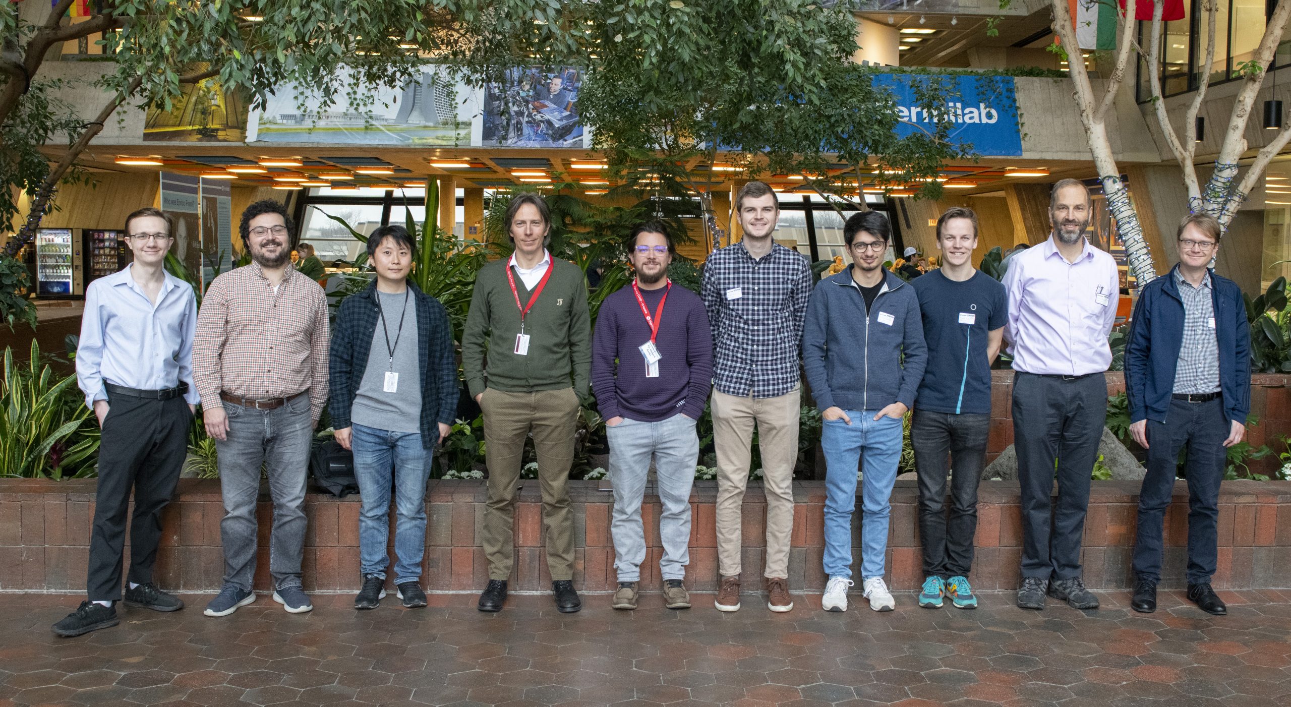
Members of the Fermilab-led co-design team at their collaboration meeting in January 2023. From left to right: Adam Quinn from Fermilab; Whitney Armstrong and Sangbaek Lee from Argonne; Davide Braga and Kyle Woodworth from Fermilab; Owen Medeiros, Matteo Castellani, Reed Foster and Karl Berggren from MIT; and Matt Shaw from Jet Propulsion Lab. Photo: Lynn Johnson, Fermilab
In 2021, DOE announced a $54-million call for labs to apply for a three-year grant for fundamental microelectronics co-design research. Fermilab was one of 10 institutions to receive the award to pursue this innovative project.
“DOE is putting a conscious effort in trying to get people with different domain expertise to work together, so that they all influence each other,” said Braga, the principal investigator of the co-design team. “That’s why we brought together this collaboration, which is quite diverse,” he explained.
The design team consists of Fermilab scientists and researchers from seven other institutions, including the Massachusetts Institute of Technology and Argonne. In January 2023, the team met for the first time in person to discuss their progress.
The funded proposal aims to revolutionize cryogenic detectors able to detect single particles or photons. To this end, the team is developing two complementary classes of cryogenic detectors, one based on ultra-low-noise semiconductor sensors, and one based on superconducting nanowire single-photon detectors, or SNSPDs, that operate below minus 268 Celsius. Though “photon” is in the name, Braga explained that these detectors can detect charged particles as well.
“Now, we are trying to incorporate this technology into particle detectors for accelerators and collider experiments,” he said.
Building a better detector
There are advantages to using these superconducting detectors in the high-magnetic-field environment of a particle accelerator that arise from how a signal is generated in the sensor. When a particle — photon or otherwise — hits the superconducting nanowire, it warms the wire enough to break the superconducting state. The nanowire exhibits electrical resistance, and the resulting voltage spike is relayed to a custom microchip for signal processing before being sent to a connected computer.
This process is markedly different from more traditional detectors that rely on ionization to generate a signal: When a charged particle zips through such a detector, it knocks electrons off atoms in its way. This causes an electric signal that is detected, amplified and ultimately sent to a computer.
Because the motion of electrons and ions is affected by the pull of high magnetic fields, ionization detectors, or charge-collection-based detectors, don’t work well inside accelerator tunnels where high-powered magnets shape particle beams. Superconducting detectors, however, may fill that niche.
“One thing that I really want to do is to push the idea of integrating superconducting detectors into the cold mass of superconducting magnets, especially for the Electron-Ion Collider,” said Armstrong. This future collider will smash electrons into ions, like the proton, to probe the inner 3D structure of the particles.
There are no other detectors that can effectively operate in those high magnetic fields and low temperatures, he explained, and this new technology could help researchers tune their accelerators more efficiently and accurately. And, in general, these detectors just work well. “They have excellent position and time resolution, and radiation hardiness,” Armstrong said.
Although typically viewed as disadvantageous, working at cryogenic temperatures may be a boon for new nuclear and particle physics applications. “It’s not necessarily very difficult for accelerators to get to liquid-helium temperatures,” he said.
The microelectronics co-design team’s device has three different components to develop and perfect: a specialized microchip; an interfacing layer of superconducting electronics; and a superconducting nanowire sensor, all three operating at a few degrees above absolute zero. Each component is being tackled by a different group on the team.
Cool microchips
Braga is the leader of the application-specific integrated circuit, or ASIC, development team designing the chips for the final device. Normal chip-integrated circuits, or microchips, operate around room temperature, said Braga, though sometimes they’re heated to 100 degrees C or cooled to minus 40 degrees C for industrial applications. It is a far cry from the researchers’ target operating temperature of minus 269 degrees C, the temperature at which helium becomes a liquid and the working temperature of the rest of the device.
“It’s not straightforward to design and operate a complex circuit at that temperature,” Braga said, “and there are no good models of how the transistors behave at that temperature.”
Yet it is important for the detector’s performance that the microchip operates as close as physically possible to the sensor. As the chip moves further away from the sensor, the device’s performance decreases, and it becomes more difficult to make the detector larger while retaining its desirable qualities.
Braga’s team, the Fermilab microelectronics group, specializes in designing high-performance, custom integrated circuits for extreme environments. It is currently developing a set of transistor models necessary to optimize the power and performance for this system.
“Everything that you do at minus 269 degrees C has to be very low power,” he explained. Having a good model helps minimize the amount of guess-and-check work that goes into developing a reliable and optimized microchip. Making the chips is expensive, Braga said, so “it’s important to have good models so that we’re confident in the performance before we go to manufacture.”
The model used by the team has paid off — the ASIC team is testing several promising prototypes now.
The challenge of cryogenic circuits
A few states away at MIT in Boston, Karl Berggren, professor of electrical engineering, leads a team of graduate students in designing and building the circuitry that will connect the cryoASIC chip designed at Fermilab to the Argonne lab sensor. But it’s not a simple plug-and-play; the MIT group will build the circuitry from the same superconducting nanowire material used on the detector.
“One of the challenges with this technology is that it’s very nascent,” said Reed Foster, a graduate student working on designing the system. “Researchers haven’t wrung out how specific design factors exactly impact the performance of the circuits that we build with these nanowires,” he said.
It means every circuit they build must be carefully tested to ensure it’s functioning as expected.
Foster explained that normally they test circuits by building a smaller circuit nested in the overall design. Self-tests from the smaller circuit let a user know if the whole circuit is functioning properly. “Currently, we’re not able to do that,” Foster said. Instead, they must couple the superconducting cryogenic circuits to room temperature circuits and use the room temperature circuits to self-test.
These two devices are not easy to combine. Although a huge benefit of superconducting circuits is how quickly information travels through them, this process requires very high-speed room temperature circuits, which are costly and can usually only test a few circuits at a time. Their first prototype can test eight circuits simultaneously, Foster said, but he plans to scale that up to 16 or more. While they continue to hammer out how to integrate a self-testing circuit into the final design, Foster’s room temperature setup will continue to ensure that the circuits work properly.
Developing cryogenic sensors
Back in Illinois, at Argonne National Laboratory, Armstrong leads the Argonne team in developing the superconducting nanowire sensor. “We just wrapped up some tests at the Fermilab test beam facility,” he said, “We took the sensors that were fabricated here at Argonne, put them into a cryostat and essentially tested them with the 120 GeV proton beam to see that we can get signal.”
The sensors fabricated by the Argonne researchers are silicon wafers inlaid with a maze of nanowire. Armstrong’s team tested the detection ability of differently sized nanowires, ranging from 100 to 800 nanometers — almost 1,000 times thinner than a strand of hair. Although wider nanowires are easier to fabricate, they don’t necessarily have the same detection capabilities of thinner nanowires.
The team are still analyzing the results from the testing, but so far it looks promising, said Armstrong. “We hope to optimize the sensor design for particle detectors at the Electron-Ion Collider,” he said.
Now they can start focusing their efforts toward scaling up the sensors.
Ultimately, these three components will be combined into a fully functioning device capable of detecting particles at liquid-helium temperatures.
“I think that, in the future, there’s going to be a large number of users of this technology,” said Armstrong.
Fermi National Accelerator Laboratory is supported by the Office of Science of the U.S. Department of Energy. The Office of Science is the single largest supporter of basic research in the physical sciences in the United States and is working to address some of the most pressing challenges of our time. For more information, please visit science.energy.gov.
Recommended reading
Using AI, Fermilab researcher probes how transistors behave in extreme cold
Olivia Seidel’s work draws on Fermilab’s deep expertise in microelectronics and cryogenic devices to support key goals of the Genesis Mission — a sweeping U.S. Department of Energy artificial intelligence initiative.
Fermilab leads multi-lab AI initiative to accelerate design of chips used in extreme environments
Researchers with Department of Energy national laboratories are working together alongside industry collaborators to support Genesis Mission goals by using the power of artificial intelligence to significantly reduce design times of custom computer chips for use in extreme temperature, high-radiation and ultra-fast environments.
New electronically tunable quantum detector speeds up search for dark matter
Scientists designed a state-of-the-art detector to electronically tune itself, enabling scientists to search broader frequency ranges for evidence of weak signals produced by dark photons — possible dark matter particles — much faster and more precisely than ever before.