Editor’s note: This article was published jointly with Argonne National Laboratory.
With a powerful enough light, you can see things that people once thought would be impossible. Large-scale light source facilities generate that powerful light, and scientists use it to create more durable materials, build more efficient batteries and computers, and learn more about the natural world.
When it comes to building these massive facilities, space is money. If you can get higher-energy beams of light out of smaller devices, you can save millions on construction costs. Add to that the chance to significantly improve the capabilities of existing light sources, and you have the motivation behind a project that has brought scientists at three U.S. Department of Energy national laboratories together.
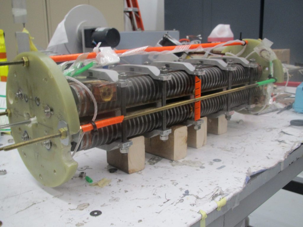
This team has just achieved an important milestone that has been in the works for more than 15 years: They have designed, built and fully tested a new state-of-the-art half-meter-long prototype magnet that meets the requirements for use in existing and future light source facilities.

This half-meter-long prototype of a niobium-tin superconducting undulator magnet was designed and built by a team from three U.S. Department of Energy national laboratories. The next step will be to build a meter-long version and install it at the Advanced Photon Source at Argonne. Photo: Ibrahim Kesgin, Argonne National Laboratory
The next step, according to Efim Gluskin, a distinguished fellow at DOE’s Argonne National Laboratory, is to scale this prototype up, build one that is more than a meter long, and install it at the Advanced Photon Source, a DOE Office of Science User Facility at Argonne. But while these magnets will be compatible with light sources like the APS, the real investment here, he said, is in the next generation of facilities that have not yet been built.
“The real scale of this technology is for future free-electron laser facilities,” Gluskin said. “If you reduce the size of the device, you reduce the size of the tunnel, and if you can do that you can save tens of millions of dollars. That makes a huge difference.”
That long-term goal brought Gluskin and his Argonne colleagues into collaboration with scientists from Lawrence Berkeley National Laboratory and Fermi National Accelerator Laboratory, both DOE labs. Each lab has been pursuing superconducting technology for decades and has in recent years focused research and development efforts on a compound that combines niobium with tin.
This material remains in a superconducting state – meaning it offers no resistance to the current running through it – even as it generates high magnetic fields, which makes it perfect for building what are called undulator magnets. Light sources like the APS generate beams of photons (particles of light) by siphoning off the energy given off by electrons as they circulate inside a storage ring. The undulator magnets are the devices that convert that energy to light, and the higher a magnetic field you can generate with them, the more photons you can create from the same size device.
There are a few superconducting undulator magnets installed at the APS now, but they are made of a niobium-titanium alloy, which for decades has been the standard. According to Soren Prestemon, senior scientist at Berkeley Lab, niobium-titanium superconductors are good for lower magnetic fields – they stop being superconducting at around 10 teslas. (That’s about 8,000 times stronger than your typical refrigerator magnet.)
“Niobium-3-tin is more complicated material,” Prestemon said, “but it is capable of transporting current at a higher field. It is superconductive up to 23 tesla, and at lower fields it can carry three times the current as niobium-titanium. These magnets are kept cold at 4.2 Kelvin, which is about minus 450 degrees Fahrenheit, to keep them superconducting.”
Prestemon has been at the forefront of Berkeley’s niobium-3-tin research program, which began back in the 1980s. The new design, developed at Argonne, built on the previous work of Prestemon and his colleagues.
“This is the first niobium-3-tin undulator that has both met the design current specifications and been fully tested in terms of magnetic field quality for beam transport,” he said.
Fermilab started working with this material in the 1990s, according to Sasha Zlobin, who initiated and led the niobium-3-tin magnet program there. Fermilab’s niobium-3-tin program has centered on superconducting magnets for particle accelerators, like the Large Hadron Collider at CERN in Switzerland and the upcoming PIP-II linear accelerator, to be built on the Fermilab site.
“We’ve demonstrated success with our high-field niobium-3-tin magnets,” Zlobin said. “We can apply that knowledge to superconducting undulators based on this superconductor.”
Part of the process, according to Emanuela Barzi, Fermilab senior scientist and co-investigator for the project, has been learning how to avoid premature quenches in the magnets as they approach the desired level of magnetic field. When the magnets lose their ability to conduct current without resistance, the resulting backlash is called a quench, and it eliminates the magnetic field and can damage the magnet itself.
The team will report in the IEEE Transactions on Applied Superconductivity that their new device accommodates nearly twice the amount of current with a higher magnetic field than the niobium-titanium superconducting undulators currently in place at the APS.
The project drew on Argonne’s experience building and operating superconducting undulators and Berkeley and Fermilab’s knowledge of niobium-3-tin. Fermilab helped to guide the process, advising on the selection of superconducting wire and sharing recent developments in their technology. Berkeley designed a state-of-the-art system that uses advanced computing techniques to detect quenches and protect the magnet.
At Argonne, the prototype was designed, fabricated, assembled and tested by a group of engineers and technicians under the guidance of Project Manager Ibrahim Kesgin, with contributions in the design, construction and testing by members of the APS superconducting undulator team led by Yury Ivanyushenkov.
The research team plans to install their full-sized prototype, which should be finished next year, at Sector 1 of the APS, which makes use of higher-energy photon beams to peer through thicker samples of material. This will be a proving ground for the device, showing that it can operate at design specifications in a working light source. But the eye, Gluskin says, is on transferring both technologies, niobium titanium and niobium-3-tin, to industrial partners and manufacturing these devices for future high-energy light source facilities.
“The key has been steady and persistent work, supported by the labs and DOE research and development funds,” Gluskin said. “It has been incremental progress, step by step, to get to this point.”
Fermilab is supported by the Office of Science of the U.S. Department of Energy. The Office of Science is the single largest supporter of basic research in the physical sciences in the United States and is working to address some of the most pressing challenges of our time. For more information, please visit energy.gov/science.


