
A collaborative research team comprised of U.S. Department of Energy national laboratories and led by Fermi National Accelerator Laboratory aims to revolutionize custom microelectronics design by using artificial intelligence to accelerate development of chips that can function in extreme environments.
The Accelerating eXtreme Environment Specs-to-Silicon — or AXESS — project will boost innovation and national competitiveness, enabling breakthroughs in quantum computing, fusion energy and particle physics.
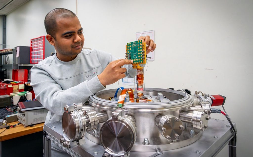
AXESS is a collaborative endeavor leveraging the strengths of the vast DOE lab complex — including Oak Ridge National Laboratory, Lawrence Berkeley National Laboratory, SLAC National Accelerator Laboratory and Sandia National Laboratories — as well as university collaborators and leading industry partners such as Siemens.
The team is developing proofs of concept for DOE’s Genesis Mission — a national mission to accelerate science through AI.
Fermilab, America’s particle physics and accelerator laboratory, is well-suited to lead this type of work and extend the adoption of rapid chip design to other research areas.
All of this coming together within the Genesis Mission is a great opportunity for Fermilab to team up with others and use AI to significantly accelerate chip design.”
Nhan Tran, head of Fermilab’s AI Program
“Particle detectors must function in some of the most extreme environments in terms of radiation, cryogenic temperatures and speed,” said Nhan Tran, head of Fermilab’s AI Program. “As a result, we’ve built our own custom detectors for many years, and Fermilab has established deep expertise in microelectronics for extreme environments. More recently, we’ve developed tools and methods used across the community to integrate AI onto chips. All of this coming together within the Genesis Mission is a great opportunity for Fermilab to team up with others and use AI to significantly accelerate chip design.”
Custom-designing specialized chips that are critical to scientific research is a highly iterative, time-intensive process that can take many months — even years — to complete.
Through this proposed Genesis Mission project, the research team is building a framework that uses AI to speed up the chip-design process, dramatically reducing the time from chip specification to fabrication from months to weeks.
“The goal of this framework is to create systems in AI that help designers make the right decisions at each step of the design process, providing feedback for the next set of designers along the pipeline,” said Giuseppe Di Guglielmo, a principal engineer at Fermilab who is co-leading the project.
Traditionally, chips are designed independently in stages, each by a different set of experts. From materials used, transistor and circuit designs, chip architecture, and finally, algorithms that run on the chips, a decision made in one stage might create issues in subsequent stages. Furthermore, the tools used are typically slow and manually operated.
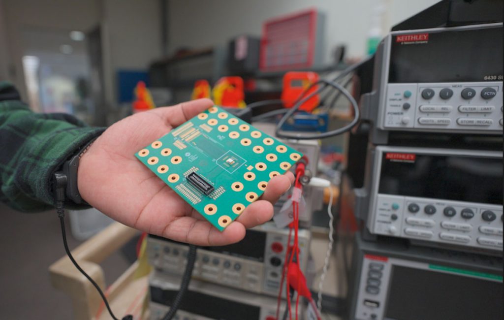
In contrast, researchers on this project are using AI to integrate all stages, ensuring any decision made in one stage optimizes the entire design and opens up traditional bottlenecks. They use one type of AI — large language models — to coordinate and automate manual steps and make high-level decisions, while another type — smaller surrogate models — act as stand-ins for the more complex and time-consuming models.
These surrogate AI models rapidly make predictions, such as how fast the chip will operate, the amount of power it will consume, the performance of the transistors, and so on, through the various stages. Within minutes, they evaluate millions of design options, predict the performance of each and isolate the most promising candidates before sending them through the full design process.
The initial proof of concept is focused on chips used to control quantum sensors, devices and systems. The team has achieved an approximately 500-times speedup for the design phase of the qubit readout algorithm and its implementation as firmware for field-programmable gate arrays. In addition, they have also developed more accurate transistor modeling at 4 kelvin — about minus 450 degrees Fahrenheit — important for operation in quantum environments. Another important area they are studying is radiation-hardened chips for use in high-energy particle physics experiments.
Under the auspices of the Genesis Mission, the researchers hope to expand this effort into a multi-year project.
By uniting Siemens’ proven technologies with the breakthrough science at Fermilab and across the DOE labs, we’re accelerating a new class of chips for quantum, fusion and high-radiation environments — at a speed and scale the nation has never had.”
David Burnette, engineering director at Siemens
“Siemens is putting industrial-grade hardware design solutions behind the Genesis Mission,” said David Burnette, engineering director for Catapult High-Level Synthesis, Siemens Digital Industries Software. “By uniting Siemens’ proven technologies with the breakthrough science at Fermilab and across the DOE labs, we’re accelerating a new class of chips for quantum, fusion and high-radiation environments — at a speed and scale the nation has never had.”
“We are really excited to be able to partner with other DOE labs and industries that have strong and complementary capabilities, bringing all these experts together across microelectronics and AI to make a big push forward for national success,” said Tran.
Fermi National Accelerator Laboratory is America’s national laboratory for particle physics and accelerator research. Fermi Forward Discovery Group manages Fermilab for the U.S. Department of Energy Office of Science. Visit Fermilab’s website at www.fnal.gov and follow us on social media
Recommended reading
DOE selects Fermilab-led AI initiative to advance particle accelerator performance
In a project selected for funding by the Department of Energy’s Genesis Mission, Fermi National Accelerator Laboratory and partners from other national laboratories, universities and industry will apply artificial intelligence and machine learning to enable precise and adaptive resonance control in particle accelerators. Their work aims to lower operating costs by millions of dollars each year and improve accelerator performance, driving scientific discovery.

DUNE uses AI to transform the future of neutrino research
DUNE is pioneering the future of neutrino research by integrating artificial intelligence into its experiment, drawing on decades of machine learning work at Fermilab.

U.S. Department of Energy invests in Fermilab projects to accelerate AI-enabled scientific discovery
The awards will support Fermilab projects by leveraging AI to boost innovation and technology development, advance DOE’s Genesis Mission and accelerate scientific discovery.